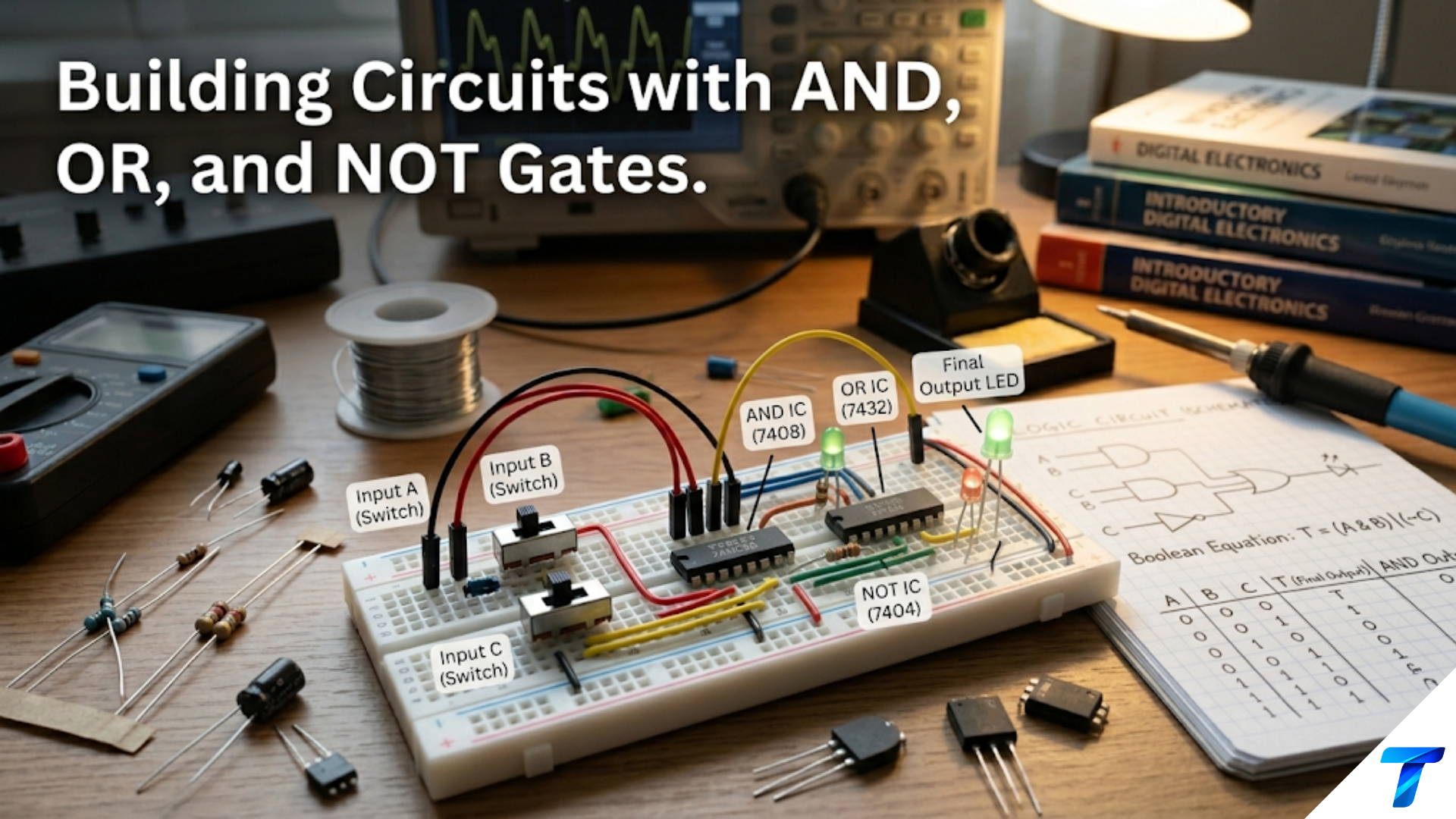
Logic gates are the fundamental building blocks of all digital electronics — simple circuits that take one or more binary inputs (HIGH or LOW, representing 1 or 0) and produce a single binary output according to a fixed logical rule. The AND gate outputs HIGH only when all inputs are HIGH. The OR gate outputs HIGH when any input is HIGH. The NOT gate inverts its single input. Every digital system — from a basic alarm circuit to a microprocessor with billions of transistors — is built entirely from combinations of these elementary operations.
Introduction: From Analog to Digital
The physical world is analog. Temperature varies continuously from −273°C to thousands of degrees. Voltage glides smoothly from one level to another. Sound pressure ripples in infinitely graduated waves. For most of human history, machines that processed information worked with these continuous quantities — analog calculators, slide rules, analog computers, vacuum tube amplifiers that faithfully reproduced every nuance of a continuously varying signal.
Digital electronics makes a radical simplification: it represents all information using only two values. Everything is either a 0 or a 1, LOW or HIGH, off or on. At first this seems like a drastic loss of precision. In practice it produces something more valuable: perfect reliability. A circuit that only needs to distinguish between two states can be built with enormous noise immunity — as long as a signal is “close enough” to HIGH, it counts as HIGH. Noise, component variation, temperature drift, and aging all become irrelevant as long as they do not push a signal across the decision boundary.
This binary representation extends to all information. Numbers become sequences of 0s and 1s in binary. Text becomes sequences of binary-coded characters. Images become grids of binary pixel values. Instructions for a processor become binary opcodes. Once everything is encoded in binary, the same basic operations apply universally to all of it.
Logic gates are the physical implementation of binary operations. They take binary inputs and produce binary outputs according to precise mathematical rules described by Boolean algebra — the algebra of true and false, 1 and 0, devised by George Boole in 1854. The AND gate implements logical conjunction. The OR gate implements logical disjunction. The NOT gate implements logical negation. From just these three fundamental operations, any conceivable logical or arithmetic function can be constructed.
Understanding logic gates — how they work electrically, what rules they follow, how they are combined, and how they are implemented in real integrated circuits — is the single most important foundation for understanding all of digital electronics. Every flip-flop, counter, adder, multiplexer, memory, and processor you will ever encounter is built from logic gates at the lowest level.
This article builds that foundation completely: the binary number system and logic levels, detailed treatment of every major gate type with truth tables and symbols, the CMOS transistor implementation that makes gates practical, the 74HC logic family ICs used throughout digital design, the essential rules for reliable circuit construction, and a series of practical design examples that combine gates into useful real-world circuits.
Binary Logic: The Two-State World
Why Two States?
Digital electronics uses two voltage levels to represent logical 0 and logical 1. In the most common CMOS logic:
- Logic LOW (0): Voltage near 0V (ground). Typically 0V to V_IL (maximum low input threshold).
- Logic HIGH (1): Voltage near V_supply. Typically V_IH (minimum high input threshold) to V_supply.
For the 74HC family at 5V supply:
- Logic LOW output: guaranteed below 0.1V
- Logic HIGH output: guaranteed above 4.4V
- Logic LOW input threshold (V_IL): anything below 1.0V is read as LOW
- Logic HIGH input threshold (V_IH): anything above 3.5V is read as HIGH
The gap between 0.1V (guaranteed LOW output) and 1.0V (LOW input threshold) gives a noise margin of 0.9V on the LOW side. The gap between 4.4V (guaranteed HIGH output) and 3.5V (HIGH input threshold) gives a noise margin of 0.9V on the HIGH side. Any noise up to 0.9V in amplitude is absorbed without causing a wrong logic reading. This noise immunity is why digital circuits are so reliable in electrically noisy environments.
Binary Numbers
Binary uses base-2 counting. Each digit position represents a power of 2:
| Binary | Decimal | Powers |
|---|---|---|
| 0001 | 1 | 2⁰ = 1 |
| 0010 | 2 | 2¹ = 2 |
| 0100 | 4 | 2² = 4 |
| 1000 | 8 | 2³ = 8 |
| 1010 | 10 | 8+2 |
| 1111 | 15 | 8+4+2+1 |
| 10000 | 16 | 2⁴ = 16 |
An N-bit binary number can represent 2^N distinct values (0 through 2^N − 1). A 4-bit number: 16 values (0–15). An 8-bit byte: 256 values (0–255). A 32-bit word: over 4 billion values.
Boolean Algebra Basics
Boolean algebra uses the same notation as ordinary algebra but with two special rules:
- Variables can only take values 0 or 1
- Addition (OR) follows: 1 + 1 = 1 (not 2)
The three fundamental operations:
- AND: written A · B or AB. Result is 1 only when both A=1 AND B=1.
- OR: written A + B. Result is 1 when A=1 OR B=1 OR both.
- NOT: written Ā or A’. Result is the opposite of A.
Key identities used constantly in digital design:
A · 0 = 0           A + 0 = A
A · 1 = A           A + 1 = 1
A · A = A           A + A = A
A · Ā = 0 A + Ā = 1De Morgan’s laws (essential for simplifying circuits):
-(A · B) = Ā + B̄     (NOT of AND = OR of NOTs)
-(A + B) = Ā · B̄ (NOT of OR = AND of NOTs)Memory aid: “Break the bar, change the sign.” When distributing a NOT over a multi-variable expression, change every AND to OR or every OR to AND.
The NOT Gate (Inverter)
Function and Truth Table
The NOT gate is the simplest gate — one input, one output, one rule: the output is always the opposite of the input.
| Input A | Output Q = Ā |
|---|---|
| 0 | 1 |
| 1 | 0 |
Schematic Symbol
A triangle (indicating a buffer/amplifier direction) with a small circle (bubble) at the output. The bubble is the universal symbol for inversion — it appears on many gate types to indicate active-LOW or inverted behavior.
A ──▷○── QThe triangle points toward the output. The circle at the tip indicates inversion.
CMOS Implementation
At the transistor level, a CMOS inverter uses exactly two transistors: one PMOS (P-channel MOSFET) connected between V_supply and the output, and one NMOS (N-channel MOSFET) connected between the output and GND. Both gates connect to the same input:
When A = LOW (0V):
- PMOS gate is LOW → PMOS turns ON (PMOS turns on when gate is LOW) → output pulled to V_supply (HIGH)
- NMOS gate is LOW → NMOS turns OFF → output disconnected from GND
When A = HIGH (V_supply):
- PMOS gate is HIGH → PMOS turns OFF → output disconnected from V_supply
- NMOS gate is HIGH → NMOS turns ON → output pulled to GND (LOW)
In both states, exactly one transistor is on and one is off — output is always driven to a definite rail. In steady state, the path from supply to ground through both transistors is broken — zero static current. This is why CMOS is so power-efficient: static power consumption is essentially zero.
Practical IC: 74HC04 Hex Inverter
The 74HC04 contains six independent NOT gates in a 14-pin DIP or SOIC package:
- Supply voltage: 2V to 6V (works at both 3.3V and 5V)
- Propagation delay: ~7ns at 5V
- Output drive: ±25mA (can source and sink substantial current)
- Pin layout: 1A→1Y, 2A→2Y, 3A→3Y (left side); 4A→4Y, 5A→5Y, 6A→6Y (right side); VCC pin 14, GND pin 7
Applications of the NOT gate:
- Signal inversion (convert active-HIGH to active-LOW)
- Non-inverting buffer (two NOT gates in series)
- Oscillator (odd number of NOT gates in a ring: output feeds back to input — no stable state, oscillates)
- Schmitt trigger variant (74HC14 — same pinout, adds hysteresis for noise immunity)
The AND Gate
Function and Truth Table
The AND gate outputs HIGH only when ALL inputs are simultaneously HIGH. One LOW input dominates — output goes LOW regardless of all other inputs.
Two-input AND:
| A | B | Q = A · B |
|---|---|---|
| 0 | 0 | 0 |
| 0 | 1 | 0 |
| 1 | 0 | 0 |
| 1 | 1 | 1 |
Output is HIGH in exactly one row. For an N-input AND, only 1 of 2^N input combinations produces a HIGH output.
Schematic Symbol
Flat input side, curved (D-shaped) output side:
    ____
A ─|    \
   |     )── Q
B ─|____/The D-shape distinguishes AND from OR (which has a curved input side and pointed output).
Physical Intuition
AND implements the logical meaning of “and” precisely. A security system should trigger when the door is open AND the alarm is armed — both conditions simultaneously. A machine should run when power is on AND the safety guard is closed AND the operator presence sensor is active.
Series switches implement AND physically: current flows only when switch 1 AND switch 2 AND switch 3 are all closed.
CMOS Implementation
A CMOS AND gate requires more transistors than NOT alone — it is actually a NAND gate (4 transistors) followed by an inverter (2 transistors) = 6 transistors total. This is why NAND is more fundamental than AND in CMOS technology, as we will see.
Practical ICs
- 74HC08: Quad 2-input AND (four AND gates, 14-pin package)
- 74HC11: Triple 3-input AND
- 74HC21: Dual 4-input AND
The OR Gate
Function and Truth Table
The OR gate outputs HIGH when ANY input is HIGH. All inputs must be LOW simultaneously to produce a LOW output.
Two-input OR:
| A | B | Q = A + B |
|---|---|---|
| 0 | 0 | 0 |
| 0 | 1 | 1 |
| 1 | 0 | 1 |
| 1 | 1 | 1 |
Output is LOW in exactly one row. For an N-input OR, only 1 of 2^N combinations (all zeros) produces a LOW output.
Schematic Symbol
Curved input side (concave arc), pointed output:
    ____
A ─\    \
    )     >── Q
B ─/____/The curved input side and pointed tip distinguish OR from AND.
Physical Intuition
Parallel switches implement OR physically: current flows when switch 1 OR switch 2 (or both) are closed. A building’s fire alarm system sounds when any detector triggers — an OR of all sensor inputs.
Practical ICs
- 74HC32: Quad 2-input OR (the most common OR gate IC)
- 74HC4075: Triple 3-input OR
The NAND Gate
Why NAND Is More Important Than AND
In CMOS silicon, the NAND gate is the natural primitive operation — it uses fewer transistors than AND (4 vs 6) and switches faster. The vast majority of logic in real ICs is implemented using NAND gates internally. NAND is also universal: any other gate can be built from NAND gates alone, making a single NAND IC sufficient to implement any logic function.
Function and Truth Table
NAND = NOT AND. Output is the complement of an AND gate:
| A | B | Q = ̄(A·B) |
|---|---|---|
| 0 | 0 | 1 |
| 0 | 1 | 1 |
| 1 | 0 | 1 |
| 1 | 1 | 0 |
Output is LOW only when ALL inputs are HIGH. Output defaults HIGH — it takes all inputs HIGH to pull it LOW.
Schematic Symbol
AND body (D-shape) with an output bubble:
    ____
A ─|    \
   |     )○── Q
B ─|____/
CMOS Implementation (4 Transistors)
Two PMOS transistors in parallel (pull-up network) and two NMOS transistors in series (pull-down network):
- When any input is LOW: The corresponding PMOS turns on (PMOS is on when gate is LOW), pulling output HIGH. The series NMOS chain is broken (at least one NMOS off), so output cannot be pulled LOW. Q = HIGH ✓
- When all inputs are HIGH: All PMOS turn off, disconnecting supply. All NMOS turn on, creating a series path to GND. Q = LOW ✓
This parallel PMOS / series NMOS structure is more efficient than the series PMOS / parallel NMOS structure of NOR, which is why NAND is faster in CMOS.
NAND Universality
Any gate can be built from NAND gates alone:
NOT from NAND: Connect both inputs together. NAND(A,A) = ̄(A·A) = ̄A ✓
AND from NAND: NAND followed by NAND-as-NOT. Two NANDs.
OR from NAND: By De Morgan: A+B = ̄(̄A·̄B) = NAND(NOT A, NOT B) = NAND(NAND(A,A), NAND(B,B)). Three NANDs.
XOR from NAND: Four NANDs in a specific configuration. (Covered in detail in Article 82.)
This universality means a designer who stocks only 74HC00 (quad NAND) can build any logic circuit.
Practical ICs
- 74HC00: Quad 2-input NAND — the single most important logic IC; know its pinout by heart
- 74HC10: Triple 3-input NAND
- 74HC20: Dual 4-input NAND
- 74HC132: Quad 2-input NAND with Schmitt trigger inputs (adds hysteresis for noise immunity)
74HC00 Pinout (14-pin DIP):
Pins 1,2 → 3  (Gate 1: A,B → Y)
Pins 4,5 → 6  (Gate 2: A,B → Y)
Pins 9,10 → 8 (Gate 3: A,B → Y)
Pins 12,13 → 11 (Gate 4: A,B → Y)
Pin 7: GND Pin 14: VCCThe NOR Gate
Function and Truth Table
NOR = NOT OR. Output is the complement of an OR gate:
| A | B | Q = ̄(A+B) |
|---|---|---|
| 0 | 0 | 1 |
| 0 | 1 | 0 |
| 1 | 0 | 0 |
| 1 | 1 | 0 |
Output is HIGH only when ALL inputs are LOW. Output defaults LOW — all inputs must be LOW to produce a HIGH.
Schematic Symbol
OR body with output bubble:
    ____
A ─\    \
    )     >○── Q
B ─/____/
NOR is Also Universal
By De Morgan’s law, NOR gates can implement any other gate:
- NOT from NOR: NOR(A,A) = ̄(A+A) = ̄A ✓
- OR from NOR: Two NORs (NOR followed by NOR-as-NOT)
- AND from NOR: NOR(NOT A, NOT B) = ̄(Ā+B̄) = A·B. Three NORs.
CMOS NOR
Two PMOS in series (pull-up) and two NMOS in parallel (pull-down). The series PMOS path is slower and weaker than NAND’s series NMOS path (PMOS has lower current drive than NMOS of the same size). This is why NOR gates are generally slower than equivalent NAND gates in CMOS — NAND is preferred when speed matters.
Practical ICs
- 74HC02: Quad 2-input NOR — note the different pinout from 74HC00! NOR ICs list output first: Y,A,B per gate, not A,B,Y.
- 74HC27: Triple 3-input NOR
The XOR Gate (Exclusive-OR)
Function and Truth Table
XOR outputs HIGH when its inputs DIFFER — when an odd number of inputs are HIGH.
| A | B | Q = A ⊕ B |
|---|---|---|
| 0 | 0 | 0 |
| 0 | 1 | 1 |
| 1 | 0 | 1 |
| 1 | 1 | 0 |
“Exclusive” OR: A or B but not both.
Schematic Symbol
OR body with an extra curved line on the input side:
    ____
A ─\)   \
    )     >── Q
B ─/)___/
The double curve on the input side is the visual key distinguishing XOR from OR.
XOR’s Unique Properties
XOR has remarkable mathematical properties that make it appear throughout digital design:
Self-inverse: (A ⊕ B) ⊕ B = A. XOR’ing twice with the same value returns the original. Foundation of reversible encryption.
Controlled NOT: A ⊕ 0 = A (passes unchanged); A ⊕ 1 = Ā (inverts). XOR with a control bit is a programmable inverter.
Parity computation: XOR of multiple bits is 1 when an odd number of bits are 1 — exactly the even parity bit calculation.
Binary addition: XOR computes the sum bit of two binary digits without carry. (AND computes the carry.) Together, XOR + AND form the half adder.
Practical ICs
- 74HC86: Quad 2-input XOR
The XNOR Gate (Exclusive-NOR / Equivalence)
Function and Truth Table
XNOR outputs HIGH when inputs are the SAME — it is an equality detector.
| A | B | Q = ̄(A⊕B) |
|---|---|---|
| 0 | 0 | 1 |
| 0 | 1 | 0 |
| 1 | 0 | 0 |
| 1 | 1 | 1 |
Output HIGH when A equals B. Used in magnitude comparators, address decoders, and key-match circuits.
Schematic Symbol
XOR body with output bubble.
Gate Summary Table
| Gate | Function | Output HIGH when… | Output LOW when… | Symbol key |
|---|---|---|---|---|
| NOT | Ā | Input is 0 | Input is 1 | Triangle + bubble |
| AND | A·B | All inputs are 1 | Any input is 0 | D-shape |
| OR | A+B | Any input is 1 | All inputs are 0 | Curved shape |
| NAND | ̄(A·B) | Any input is 0 | All inputs are 1 | D-shape + bubble |
| NOR | ̄(A+B) | All inputs are 0 | Any input is 1 | Curved + bubble |
| XOR | A⊕B | Inputs differ | Inputs match | Curved + extra arc |
| XNOR | ̄(A⊕B) | Inputs match | Inputs differ | Curved + arc + bubble |
The 74HC Logic Family: Practical Implementation
Why 74HC?
The 74HC (High-speed CMOS) logic family is the standard for discrete digital logic design:
- Wide supply voltage: 2V to 6V — works at 3.3V and 5V systems
- Very low power: Near-zero static current — only switching transients draw power
- High speed: Propagation delay ~7ns at 5V — fast enough for clock rates to tens of MHz
- Strong output drive: ±25mA per output — can drive LEDs, transistor bases, and multiple inputs
- Complete family: Every gate type available in compatible packages
- Inexpensive and universal: Available from every electronics supplier worldwide
3.3V Operation: 74LVC
For 3.3V systems (ESP32, STM32, Raspberry Pi), use the 74LVC family:
- Supply: 1.65V to 3.6V
- Many 74LVC devices are 5V-tolerant on inputs — they accept 5V inputs while running on 3.3V
- Same pinout as 74HC — drop-in compatible
- Example: 74LVC00 (quad NAND), 74LVC04 (hex NOT), 74LVC08 (quad AND), 74LVC32 (quad OR)
Critical Rule: Decoupling Capacitors
Every logic IC must have a 100nF ceramic capacitor between its VCC pin and GND pin, placed as close to the IC as physically possible (within 3mm).
When a logic gate switches its output, it draws a brief, large current spike from the power supply — the output capacitance charges or discharges rapidly. This spike flows through the inductance of the supply traces, creating a voltage glitch on VCC. Without a local decoupling capacitor, this glitch propagates to other ICs and causes false switching, increased EMI, and intermittent failures.
The decoupling capacitor supplies the instantaneous current locally, preventing it from flowing through the supply trace inductance. This is the single most important PCB rule for digital design. Every IC. Every time. No exceptions.
For boards with many ICs, also add a 10µF electrolytic capacitor near the power supply connector as bulk charge reserve.
Critical Rule: Handle Unused Inputs
CMOS logic inputs are high-impedance (gate oxide). An unconnected CMOS input floats at whatever voltage it picks up from nearby signals, supply noise, and electromagnetic interference. The voltage on a floating input is undefined and may settle anywhere between 0V and V_supply — in the linear region where both PMOS and NMOS are partially on simultaneously, drawing excessive current, generating heat, and producing unpredictable output.
Rule: Every unused gate input must be tied to a defined logic level:
- Unused AND gate inputs → tie to VCC (HIGH is neutral for AND: A·1 = A)
- Unused OR gate inputs → tie to GND (LOW is neutral for OR: A+0 = A)
- Unused NAND inputs → tie to VCC
- Unused NOR inputs → tie to GND
- Unused NOT inputs → tie to either level (but tie to something)
If an entire gate within an IC is unused, tie its inputs to GND and leave its output unconnected. This prevents oscillation and excessive power consumption.
Combining Gates: From Logic to Circuits
Truth Table to Gate Circuit
Any Boolean function can be implemented directly from its truth table using the Sum of Products (SoP) method:
- Identify every row where the output is 1
- For each such row, write a product term (AND of all inputs, with inputs that are 0 complemented)
- OR all the product terms together
Example: Q = 1 for inputs A=0,B=1 and A=1,B=0 (this is XOR):
- Row A=0,B=1: term = Ā·B
- Row A=1,B=0: term = A·B̄
- Q = Ā·B + A·B̄
Implemented with: 2 NOT gates + 2 AND gates + 1 OR gate = 5 gates. Or more efficiently: 1 XOR gate = 1 gate.
Always simplify before building. Karnaugh maps (K-maps, covered in Article 80) provide a systematic minimization method.
Propagation Delay and Timing
Real gates do not switch instantaneously. The propagation delay t_pd (approximately 7ns for 74HC at 5V) represents the time from when an input changes to when the output reaches its new valid level.
In a multi-level circuit (gates feeding gates), delays accumulate:
Total delay = number of gate levels × t_pd_per_gateFor 4 levels of 74HC: 4 × 7ns = 28ns. Maximum clock frequency ≤ 1/28ns ≈ 35MHz (with no additional setup time). In practice, use 2–3× safety margin: reliable operation to ~10–15MHz.
For high-speed designs, minimizing the number of gate levels in the critical path is essential. This is one of the motivations for carry-lookahead adders (which reduce carry propagation from O(N) levels to O(log N)) and other fast logic structures.
Practical Design Examples
Design Example 1: Majority Vote Safety Interlock
Application: A machine requires a majority of three independent safety sensors (A, B, C) to confirm safe operating conditions. The machine runs only when at least 2 of 3 sensors indicate safe (HIGH). A single sensor failure should not stop the machine (fault tolerance); two or more must agree that it is unsafe.
Boolean function: Q = 1 when 2 or more of A, B, C are 1.
Truth table:
| A | B | C | Q |
|---|---|---|---|
| 0 | 0 | 0 | 0 |
| 0 | 0 | 1 | 0 |
| 0 | 1 | 0 | 0 |
| 0 | 1 | 1 | 1 |
| 1 | 0 | 0 | 0 |
| 1 | 0 | 1 | 1 |
| 1 | 1 | 0 | 1 |
| 1 | 1 | 1 | 1 |
SoP expression:
Q = Ā·B·C + A·B̄·C + A·B·C̄ + A·B·CSimplification (K-map or Boolean algebra):
Group pairs that differ in one variable:
- Rows 4 and 8: B·C (A varies — eliminated)
- Rows 6 and 8: A·C (B varies — eliminated)
- Rows 7 and 8: A·B (C varies — eliminated)
Q = A·B + A·C + B·CGate implementation:
- Gate 1 (AND): A, B → A·B
- Gate 2 (AND): A, C → A·C
- Gate 3 (AND): B, C → B·C
- Gate 4 (OR, 3-input): A·B, A·C, B·C → Q
ICs: 74HC08 (quad AND, uses 3 gates) + 74HC4075 (triple 3-input OR, uses 1 gate).
Verification:
A=1, B=1, C=0: A·B=1, A·C=0, B·C=0 → Q=1 ✓ (two sensors agree safe) A=1, B=0, C=0: A·B=0, A·C=0, B·C=0 → Q=0 ✓ (only one sensor safe) A=1, B=1, C=1: A·B=1 → Q=1 ✓ (all three safe)
Design Example 2: Alarm System with Enable and Silence
Application: Security alarm with three sensors (DOOR, WINDOW, MOTION). System ARM signal enables the alarm. ACK (acknowledge) button silences. ALARM = ARM AND (any sensor active) AND NOT ACK.
Boolean expression:
TRIGGER = DOOR + WINDOW + MOTION
ALARM = ARM · TRIGGER · ACK̄Gate implementation:
- Gate 1 (OR): DOOR, WINDOW → intermediate
- Gate 2 (OR): intermediate, MOTION → TRIGGER (any sensor)
- Gate 3 (NOT): ACK → ACK̄
- Gate 4 (AND, 3-input): ARM, TRIGGER, ACK̄ → ALARM
ICs: 74HC32 (quad OR, uses 2 gates) + 74HC04 (uses 1 NOT gate) + 74HC11 (triple 3-input AND, uses 1 gate). All three ICs contribute at most 1–2 gates each — with plenty of spare gates for future additions.
Adding a LED and buzzer:
ALARM output → 470Ω → LED → GND  (LED indicates alarm)
ALARM output → 1kΩ → NPN base (BC547) → buzzer → V_supply
                      NPN emitter → GND
1N4001 flyback diode across buzzerThe 74HC gate output (±25mA) directly drives the LED. For the buzzer (which draws more current), the NPN transistor amplifies the gate’s drive capability.
Design Example 3: 2-to-4 Line Decoder
Application: A microcontroller has 2 address bits (A1, A0) selecting one of four peripheral devices. Exactly one device enable line (Y0–Y3) should be LOW (active-LOW enable) for each address combination.
Truth table:
| A1 | A0 | Y0 | Y1 | Y2 | Y3 |
|---|---|---|---|---|---|
| 0 | 0 | 0 | 1 | 1 | 1 |
| 0 | 1 | 1 | 0 | 1 | 1 |
| 1 | 0 | 1 | 1 | 0 | 1 |
| 1 | 1 | 1 | 1 | 1 | 0 |
Active-LOW outputs: each output goes LOW when its address is selected.
Expressions (active-LOW means output = complement of the AND of address bits):
Y0 = -(Ā1 · Ā0) = NAND(Ā1, Ā0)
Y1 = -(Ā1 · A0) = NAND(Ā1, A0)
Y2 = -(A1 · Ā0) = NAND(A1, Ā0)
Y3 = -(A1 · A0) = NAND(A1, A0)Each output is a NAND gate — natural for NAND logic and natural for active-LOW chip-select signals.
Gate implementation:
- 2 NOT gates: Ā0 and Ā1 (from 74HC04)
- 4 NAND gates: Y0–Y3 (from 74HC00 — uses all four gates exactly)
Verification:
A1=1, A0=0 (select device 2):
- Ā0=1, Ā1=0
- Y0 = NAND(0,1) = 1 ✓ (not selected)
- Y1 = NAND(0,0) = 1 ✓
- Y2 = NAND(1,1) = 0 ✓ (selected — LOW)
- Y3 = NAND(1,0) = 1 ✓
This is exactly what the 74HC139 (dual 2-to-4 decoder) implements internally — understanding the gate-level design reveals how all decoder ICs work.
Design Example 4: NAND SR Latch for Switch Debounce
Application: A mechanical SPDT switch bounces up to 10ms when thrown. Build a circuit that produces a clean, instantaneous transition with no bounce.
Circuit: Two NAND gates cross-coupled with active-LOW inputs (S̄ and R̄):
S̄ ─┐
    NAND1 ──────── Q
Q̄ ─┘  (feedback)

R̄ ─┐
    NAND2 ──────── Q̄
Q ─┘ (feedback)SPDT switch connections:
- Switch common → GND
- Switch position 1 → S̄ (with 10kΩ pull-up to VCC): LOW when switch is in position 1
- Switch position 2 → R̄ (with 10kΩ pull-up to VCC): LOW when switch is in position 2
Behavior when switch moves to position 1 (S̄ goes LOW):
- NAND1 sees S̄=0 → output Q=1 (regardless of feedback)
- Switch bounces: S̄ goes HIGH briefly → latch enters hold state → Q stays 1
- Switch bounces again → S̄ goes LOW → latch tries to set → Q already 1, no change
The latch responds to the FIRST contact and ignores all subsequent bounces. Output Q is clean.
Implementation: Two gates from a 74HC00. Uses only half the IC — two gates remain for other logic.
IC connections (74HC00):
Gate 1 (pins 1,2→3): pin1=S̄, pin2=Q̄(feedback from pin6), pin3=Q output
Gate 2 (pins 4,5→6): pin4=R̄, pin5=Q(feedback from pin3), pin6=Q̄ outputDesign Example 5: Parity Generator for Serial Communication
Application: Generate an even parity bit for a 4-bit data nibble before transmission. The parity bit makes the total number of 1s (including parity) always even.
Function: P = D3 ⊕ D2 ⊕ D1 ⊕ D0
XOR of all four data bits. If the count of 1s is even, P=0 (total remains even). If odd, P=1 (makes total even).
Gate implementation (tree structure):
X1 = D0 ⊕ D1   (XOR gate 1)
X2 = D2 ⊕ D3   (XOR gate 2)
P = X1 ⊕ X2 (XOR gate 3)3 XOR gates, 2 levels of logic. Tree structure minimizes depth compared to chaining four XORs linearly (which would require 3 gates but 3 levels of delay).
IC: 74HC86 (quad XOR) — uses 3 of 4 gates.
Verification:
D = 1011 (three 1s — odd):
- X1 = 1⊕1 = 0
- X2 = 0⊕1 = 1
- P = 0⊕1 = 1 → total 1s = 3+1 = 4 (even) ✓
D = 1100 (two 1s — even):
- X1 = 0⊕0 = 0
- X2 = 1⊕1 = 0
- P = 0⊕0 = 0 → total 1s = 2+0 = 2 (even) ✓
At the receiver: Recompute parity over all 5 received bits (D3–D0 + P). If result is 0: no error (even parity confirmed). If result is 1: error detected (odd parity means one bit flipped). Parity detects any single-bit error but cannot identify which bit was wrong.
Building Reliable Gate Circuits: Practical Rules
Power Supply
Use a stable, regulated 5V supply (74HC) or 3.3V supply (74LVC). Ripple on the supply rail appears directly as noise on logic signals. A 7805 linear regulator or LM3940 (5V→3.3V) works well for bench circuits. On breadboards, the supply rail resistance can cause voltage drops when multiple gates switch simultaneously — keep supply wiring short and thick.
Breadboard Construction
- Orient ICs across the center divider (legs straddle the gap)
- Immediately add the 100nF decoupling capacitor before wiring anything else
- Use short wires — long wires act as antennas and pick up noise
- Tie all unused inputs to defined levels before testing
- Color-code: red = VCC, black = GND, other colors for signals
Testing Procedure
- Check supply voltage at each IC’s VCC pin before connecting inputs
- Set all inputs through all 2^N combinations in order (binary counting pattern)
- Verify each output matches the expected truth table entry
- If behavior is incorrect: check pinout (74HC00 and 74HC02 have DIFFERENT pin layouts), check decoupling, check for floating inputs
Fan-Out and Loading
One logic gate output can drive how many inputs? For 74HC:
- Output drive: ±25mA
- Input current: < 1µA (CMOS input)
- Fan-out: 25mA / 1µA = 25,000 — effectively unlimited within a PCB
Fan-out only becomes a concern when driving non-CMOS loads (LEDs, transistors, long cables with significant capacitance). For LED drive (10mA maximum): fine, but use a series resistor. For cables (high capacitance): add a buffer gate to provide sufficient drive current for fast switching into the cable capacitance.
Common Mistakes and How to Avoid Them
Mistake 1: Floating inputs on unused gates
Left floating, CMOS inputs draw excessive current (both pull-up and pull-down transistors partially on), the output oscillates unpredictably, and adjacent circuits see noise. Always tie unused inputs to VCC or GND.
Mistake 2: Missing decoupling capacitors
Intermittent failures, sensitivity to power supply variations, excessive radiated EMI. Add 100nF ceramic directly at every IC’s VCC pin. This is not optional.
Mistake 3: Confusing 74HC00 and 74HC02 pinouts
The quad NAND (74HC00) and quad NOR (74HC02) use the same 14-pin package but different internal pin assignments. 74HC00 has each gate arranged as A,B,Y (inputs first). 74HC02 has each gate as Y,A,B (output first). They are NOT interchangeable despite looking identical. Always verify with the datasheet.
Mistake 4: Mixing logic families without voltage translation
74HC outputs at 5V (4.4V minimum HIGH) drive 74LVC inputs that may have a maximum input rating of 3.6V — the 5V signal can exceed the 74LVC’s absolute maximum input voltage. Use 74LVC devices with 5V-tolerant inputs when connecting 5V and 3.3V logic, or add a level shifter.
Mistake 5: Connecting outputs together
CMOS outputs are totem-pole (push-pull) — connecting two outputs together directly causes a shoot-through fault when one drives HIGH while the other drives LOW. Never wire CMOS outputs together. Use tri-state outputs or open-drain/open-collector outputs (like 74HC03 open-drain NAND) for bus applications.
Mistake 6: Expecting AND/OR when you need NAND/NOR
In many practical circuits, active-LOW signals (common in chip-select and enable applications) combine naturally with NAND/NOR gates. A NAND gate whose output is LOW when all chip-select conditions are met (active-LOW enables) is often exactly what is needed — not an AND gate followed by a NOT. Think in terms of the signal polarity from the start.
Summary
Logic gates are the irreducible building blocks of digital electronics — simple circuits implementing the seven fundamental Boolean operations (NOT, AND, OR, NAND, NOR, XOR, XNOR) on binary signals. Each gate follows an exact rule captured in its truth table; by combining gates, any conceivable digital function can be implemented.
NOT inverts its single input. AND requires all inputs HIGH for a HIGH output. OR requires any input HIGH. NAND and NOR are the complements of AND and OR respectively — and both are universal, meaning any gate can be built from NAND alone or NOR alone. XOR detects difference between inputs; XNOR detects equality.
CMOS technology implements all these gates efficiently using complementary pairs of PMOS and NMOS transistors. NAND and NOR gates are more fundamental in CMOS than AND and OR — each requires only 4 transistors, while AND and OR each require 6. NAND gates are faster than NOR because their series NMOS pull-down path is faster than NOR’s series PMOS pull-up path.
The 74HC family provides every gate type in standardized 14-pin packages operating from 2V to 6V at ±25mA drive capability. Every circuit built from these ICs requires 100nF ceramic decoupling capacitors at every VCC pin and defined (non-floating) connections on every unused input — these are not suggestions but requirements for reliable operation.
The five design examples — majority vote safety interlock, alarm system, 2-to-4 decoder, NAND SR latch debouncer, and parity generator — demonstrate how gates combine to solve real engineering problems, from safety-critical machine control to data integrity checking in communications.