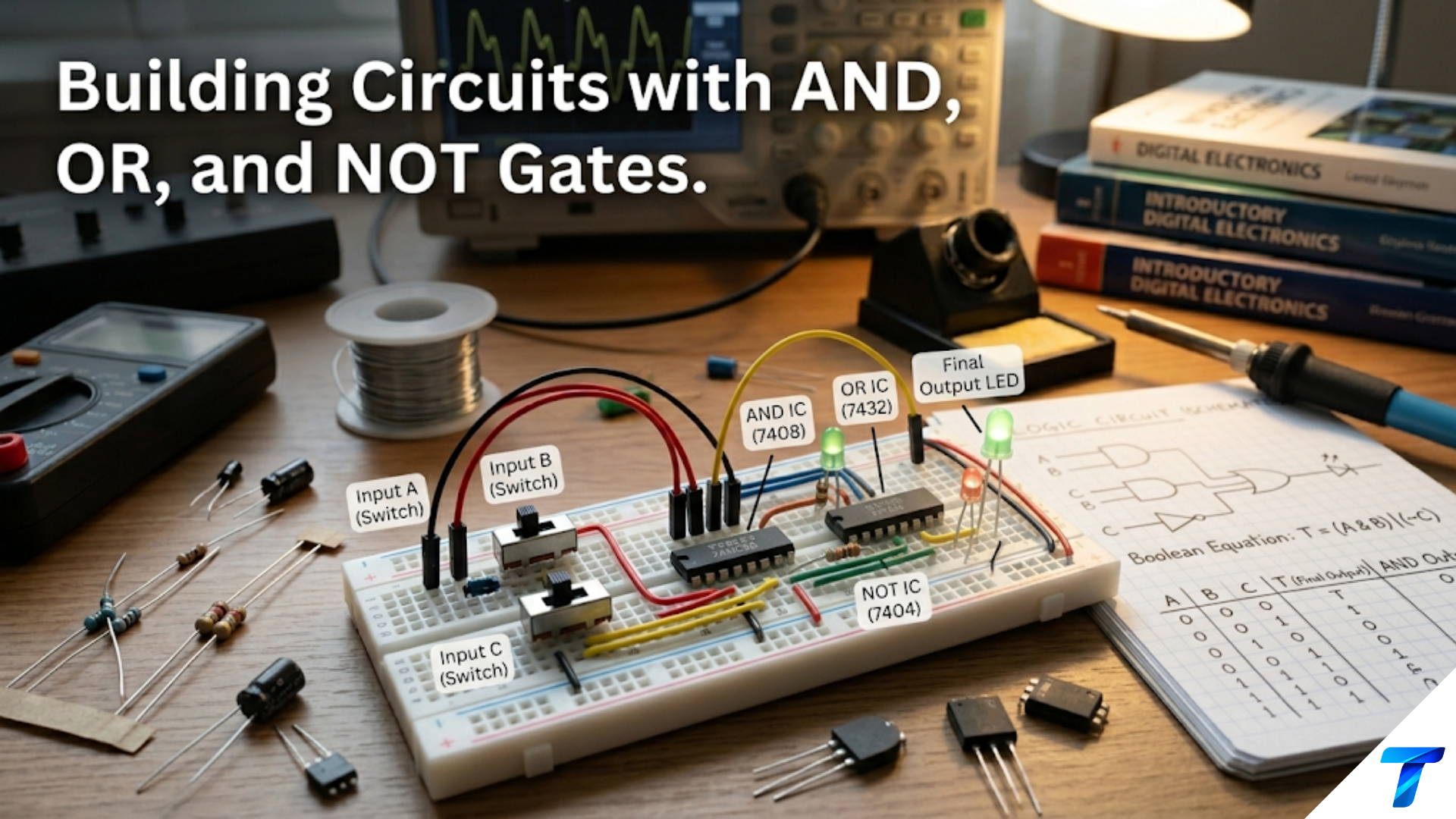
A truth table is a systematic listing of every possible combination of logic inputs alongside the corresponding output for each combination. For a circuit with N inputs, the truth table has exactly 2^N rows — one for each unique combination of 0s and 1s. Truth tables are the fundamental tool for specifying, analyzing, and verifying digital logic: they translate verbal requirements (“the alarm activates when the door is open AND the system is armed”) into a precise, unambiguous mathematical specification that can be directly converted into a gate circuit.
Introduction: Making Logic Unambiguous
Human language is wonderfully flexible and expressive, but it is also deeply ambiguous. Consider the instruction: “Sound the alarm if the door is open or the window is broken and the system is armed.” Does “armed” apply to both conditions, or just to the window? Does “or” create one condition with two parts, or two independent conditions? A security engineer reading this might implement it one way; a software developer might implement it differently; the client who wrote it might have intended a third interpretation entirely.
Digital circuits cannot tolerate this ambiguity. A logic gate does exactly one thing, always, with no room for interpretation. Before any gate is designed or any code is written, the designer needs an absolutely precise specification of what the system should do for every possible combination of inputs. This precision is what truth tables provide.
A truth table is the mathematical contract between a system’s requirements and its implementation. It lists every possible input state (all 2^N combinations for N binary inputs) and specifies, unambiguously, what the output should be for each one. Once the truth table is complete, the Boolean expression and gate circuit follow by systematic procedure — no guesswork, no ambiguity, no forgotten edge cases.
Truth tables are useful in both directions: forward (from truth table to gate circuit — design) and backward (from gate circuit to truth table — analysis and verification). A designer uses them to translate requirements into circuits. A troubleshooter uses them to predict what a circuit should do and compare that prediction to measured behavior to find faults. A student uses them to understand exactly what a new gate combination does before building it.
This article provides a complete, practical guide to truth tables and their use in digital logic design. It covers how to construct truth tables from scratch, how to derive Boolean expressions from completed truth tables using the Sum of Products (SoP) method, how to use Karnaugh maps (K-maps) to simplify those expressions to the minimum number of gates, and how to translate the simplified expression into a working circuit. Five complete design walkthroughs demonstrate the full process from verbal specification to optimized gate circuit.
Constructing a Truth Table: The Systematic Method
Step 1: Identify Inputs and Outputs
Before drawing any rows or columns, define what the system does:
- List every independent input signal and give each a letter name (A, B, C, … or descriptive names like DOOR, ARMED, TIMER)
- List every output signal that needs to be determined (Q, ALARM, ENABLE, etc.)
- Count the number of inputs: N inputs → 2^N rows in the table
For a system with:
- 1 input: 2^1 = 2 rows
- 2 inputs: 2^2 = 4 rows
- 3 inputs: 2^3 = 8 rows
- 4 inputs: 2^4 = 16 rows
- 5 inputs: 2^5 = 32 rows
- 8 inputs: 2^8 = 256 rows
The exponential growth of 2^N is why digital design focuses on minimizing inputs — adding one more input doubles the truth table size and complexity.
Step 2: Fill in the Input Columns Systematically
The input columns must list every combination exactly once. The standard method produces a binary count pattern (like counting in binary from 0 to 2^N − 1):
For 3 inputs (A, B, C):
The rightmost input (C) alternates every row: 0, 1, 0, 1, 0, 1, 0, 1 The middle input (B) alternates every 2 rows: 0, 0, 1, 1, 0, 0, 1, 1 The leftmost input (A) alternates every 4 rows: 0, 0, 0, 0, 1, 1, 1, 1
| Row | A | B | C |
|---|---|---|---|
| 0 | 0 | 0 | 0 |
| 1 | 0 | 0 | 1 |
| 2 | 0 | 1 | 0 |
| 3 | 0 | 1 | 1 |
| 4 | 1 | 0 | 0 |
| 5 | 1 | 0 | 1 |
| 6 | 1 | 1 | 0 |
| 7 | 1 | 1 | 1 |
General rule for N inputs: The column for the k-th input from the right (k = 0 for rightmost) alternates every 2^k rows. This guarantees every combination appears exactly once and in a consistent, readable order.
Verification: Read each row as a binary number (A is MSB, C is LSB): 000, 001, 010, 011, 100, 101, 110, 111 = decimal 0 through 7. All eight combinations present, none repeated. ✓
Step 3: Fill in the Output Column(s)
For each row, evaluate the output given the inputs in that row. This evaluation can come from:
A verbal specification: “The alarm activates if A is HIGH and (B OR C) is HIGH” → evaluate A · (B + C) for each row.
An existing circuit: Trace through the gate network for each input combination to determine the output.
Intuition/design intent: Directly specify what you want the output to be for each combination, then derive the circuit from the completed table.
Step 4: Verify Completeness
Count the output column entries. There should be exactly 2^N entries — one per row. Check that you have not skipped any rows or left any outputs undefined.
Truth Tables for the Basic Gates
Understanding individual gate truth tables is essential before combining them.
NOT Gate
| A | Q = Ā |
|---|---|
| 0 | 1 |
| 1 | 0 |
AND Gate (2-input)
| A | B | Q = A·B |
|---|---|---|
| 0 | 0 | 0 |
| 0 | 1 | 0 |
| 1 | 0 | 0 |
| 1 | 1 | 1 |
Output HIGH only in the last row — when A=1 AND B=1.
OR Gate (2-input)
| A | B | Q = A+B |
|---|---|---|
| 0 | 0 | 0 |
| 0 | 1 | 1 |
| 1 | 0 | 1 |
| 1 | 1 | 1 |
Output LOW only in the first row — when A=0 AND B=0.
NAND Gate (NOT-AND)
| A | B | Q = ̄(A·B) |
|---|---|---|
| 0 | 0 | 1 |
| 0 | 1 | 1 |
| 1 | 0 | 1 |
| 1 | 1 | 0 |
NAND is the inverse of AND. Output LOW only when ALL inputs are HIGH.
NOR Gate (NOT-OR)
| A | B | Q = ̄(A+B) |
|---|---|---|
| 0 | 0 | 1 |
| 0 | 1 | 0 |
| 1 | 0 | 0 |
| 1 | 1 | 0 |
NOR is the inverse of OR. Output HIGH only when ALL inputs are LOW.
XOR Gate (Exclusive-OR)
| A | B | Q = A⊕B |
|---|---|---|
| 0 | 0 | 0 |
| 0 | 1 | 1 |
| 1 | 0 | 1 |
| 1 | 1 | 0 |
Output HIGH when inputs DIFFER. Output LOW when inputs MATCH.
XNOR Gate (Exclusive-NOR, Equivalence)
| A | B | Q = ̄(A⊕B) |
|---|---|---|
| 0 | 0 | 1 |
| 0 | 1 | 0 |
| 1 | 0 | 0 |
| 1 | 1 | 1 |
Output HIGH when inputs MATCH (the opposite of XOR). Also called an equivalence gate.
Summary of Gate Behaviors
| Gate | When is output HIGH? | When is output LOW? |
|---|---|---|
| NOT | Input is 0 | Input is 1 |
| AND | All inputs are 1 | Any input is 0 |
| OR | Any input is 1 | All inputs are 0 |
| NAND | Any input is 0 | All inputs are 1 |
| NOR | All inputs are 0 | Any input is 1 |
| XOR | Inputs differ | Inputs match |
| XNOR | Inputs match | Inputs differ |
Analyzing a Circuit with a Truth Table
Given a circuit (gate network), constructing its truth table tells you exactly what the circuit does for every input combination. This is essential for verification and troubleshooting.
Example: Analyze Q = (A + B) · C̄
Step 1: Identify inputs (A, B, C) and intermediate signals. Draw 8-row table.
Step 2: Add a column for each intermediate signal: (A+B) and C̄.
Step 3: Fill in the truth table column by column:
| A | B | C | A+B | C̄ | Q = (A+B)·C̄ |
|---|---|---|---|---|---|
| 0 | 0 | 0 | 0 | 1 | 0·1 = 0 |
| 0 | 0 | 1 | 0 | 0 | 0·0 = 0 |
| 0 | 1 | 0 | 1 | 1 | 1·1 = 1 |
| 0 | 1 | 1 | 1 | 0 | 1·0 = 0 |
| 1 | 0 | 0 | 1 | 1 | 1·1 = 1 |
| 1 | 0 | 1 | 1 | 0 | 1·0 = 0 |
| 1 | 1 | 0 | 1 | 1 | 1·1 = 1 |
| 1 | 1 | 1 | 1 | 0 | 1·0 = 0 |
Reading the result: The output is HIGH when C=0 AND (A=1 OR B=1 OR both). In plain English: “Q is true when C is false and at least one of A or B is true.” This is exactly what the expression says — the truth table confirms our understanding.
Multi-Level Circuit Analysis
For circuits with many gate levels, introduce a column for every gate output. Work left to right (from inputs to output), filling each column before computing the next. The systematic column-by-column approach prevents errors that arise from trying to evaluate the whole circuit at once.
Deriving a Boolean Expression from a Truth Table: Sum of Products
Given a completed truth table (with outputs specified), derive the Boolean expression by the Sum of Products (SoP) method — also called the canonical minterm expansion.
The Sum of Products Method
Step 1: Identify all rows where the output Q = 1.
Step 2: For each HIGH-output row, write a product term (AND of all inputs):
- If an input is 1 in that row: include the input uncomplemented (A)
- If an input is 0 in that row: include the input complemented (Ā)
This product term is called a minterm — it evaluates to 1 for exactly that one row and 0 for all other rows.
Step 3: OR together all the minterms. The resulting expression equals 1 whenever any of the minterms equals 1 — which is exactly when Q = 1 in the truth table.
SoP Example
Truth table:
| A | B | C | Q |
|---|---|---|---|
| 0 | 0 | 0 | 0 |
| 0 | 0 | 1 | 1 |
| 0 | 1 | 0 | 0 |
| 0 | 1 | 1 | 1 |
| 1 | 0 | 0 | 1 |
| 1 | 0 | 1 | 0 |
| 1 | 1 | 0 | 0 |
| 1 | 1 | 1 | 1 |
Sum of minterms:
Q = Ā·B̄·C + Ā·B·C + A·B̄·C̄ + A·B·CThis expression is mathematically complete and correct — it exactly represents the truth table. But it may not be the simplest implementation. The expression uses four AND gates (3-input each) and one 4-input OR gate = 5 gates. Can we simplify?
Boolean simplification by inspection:
- Terms 1 and 2 share Ā·C: Ā·B̄·C + Ā·B·C = Ā·C·(B̄ + B) = Ā·C·1 = Ā·C
- Terms 3 and 4 do not simplify easily without a systematic method
Partly simplified: Q = Ā·C + A·B̄·C̄ + A·B·C
Better, but we can do more with a systematic tool: the Karnaugh map.
The Karnaugh Map: Systematic Minimization
The Karnaugh map (K-map), developed by Maurice Karnaugh in 1953, is a visual tool for minimizing Boolean expressions. It arranges truth table rows in a 2D grid where adjacent cells differ in exactly one variable — revealing opportunities to combine terms that Boolean algebra algebra might miss.
Two-Variable K-Map
For 2 inputs (A, B), the K-map has 2^2 = 4 cells:
        B=0    B=1
A=0  |  m0  |  m1  |
A=1 | m2 | m3 |Each cell corresponds to one truth table row (minterm). Fill in the output value (0 or 1) for each cell.
Three-Variable K-Map
For 3 inputs (A, B, C), the K-map has 8 cells arranged in a 2×4 grid. The critical rule: the column headers must follow Gray code order (00, 01, 11, 10) — not binary order — so that adjacent columns differ in only one variable:
         BC=00  BC=01  BC=11  BC=10
A=0    |   m0  |  m1  |  m3  |  m2  |
A=1 | m4 | m5 | m7 | m6 |Important: The BC columns are in Gray code order (00, 01, 11, 10) — NOT binary order (00, 01, 10, 11). This ensures adjacency between columns 11 and 10, and — crucially — the K-map wraps around: the rightmost column (BC=10) is also adjacent to the leftmost column (BC=00). Think of the K-map as wrapping into a cylinder.
Four-Variable K-Map
For 4 inputs (A, B, C, D), the K-map has 16 cells in a 4×4 grid:
            CD=00  CD=01  CD=11  CD=10
AB=00     |   m0  |  m1  |  m3  |  m2  |
AB=01     |   m4  |  m5  |  m7  |  m6  |
AB=11     |  m12  | m13  | m15  | m14  |
AB=10 | m8 | m9 | m11 | m10 |The rows also follow Gray code (00, 01, 11, 10), and the map wraps in both dimensions — top row is adjacent to bottom row, leftmost column is adjacent to rightmost column.
K-Map Grouping Rules
The minimization process finds groups of 1-cells (cells containing 1) following these rules:
Rule 1: Groups must be rectangular (including squares).
Rule 2: Group sizes must be powers of 2: 1, 2, 4, 8, or 16 cells.
Rule 3: Each group must contain only 1s (no 0s).
Rule 4: Groups may wrap around the edges (the map is toroidal — wraps in both directions).
Rule 5: A cell may belong to multiple groups.
Rule 6: Find the minimum number of groups needed to cover ALL 1s.
Rule 7: Prefer LARGER groups — a group of 4 reduces to a 1-literal term; a group of 2 reduces to a 2-literal term; a single cell remains a 3-literal minterm (for 3-variable map).
Reading the Simplified Expression from Groups
Each group of 2^k cells in an N-variable K-map simplifies to a product term with (N − k) literals:
- Group of 1 cell: N literals (no simplification — just the minterm)
- Group of 2 cells: N−1 literals (one variable eliminated)
- Group of 4 cells: N−2 literals
- Group of 8 cells: N−3 literals
To read the product term for a group:
- Identify which variables are constant within the group (same value in all cells)
- If a variable is always 0 in the group: include its complement (Ā)
- If a variable is always 1 in the group: include it uncomplemented (A)
- If a variable changes (0 in some cells, 1 in others): the variable is eliminated
The simplified Boolean expression = OR of all group product terms.
K-Map Worked Example
Truth table:
| A | B | C | Q |
|---|---|---|---|
| 0 | 0 | 0 | 1 |
| 0 | 0 | 1 | 1 |
| 0 | 1 | 0 | 0 |
| 0 | 1 | 1 | 1 |
| 1 | 0 | 0 | 1 |
| 1 | 0 | 1 | 1 |
| 1 | 1 | 0 | 0 |
| 1 | 1 | 1 | 1 |
Fill in K-map (placing Q values in cells, using minterm numbering):
           BC=00  BC=01  BC=11  BC=10
A=0    |   1(m0)| 1(m1)| 1(m3)| 0(m2)|
A=1 | 1(m4)| 1(m5)| 1(m7)| 0(m6)|Identify groups of 1s:
Group 1: The entire left two columns (BC=00 and BC=01, both rows) — a group of 4:
- Cells: m0, m1, m4, m5
- A varies (0 and 1) → eliminated
- B = 0 in all cells → include B̄
- C varies (0 and 1) → eliminated
- Term: B̄
Group 2: The top-right 1 (m3) and bottom-right 1 (m7) — a group of 2 (vertical pair in BC=11 column):
- Cells: m3, m7
- A varies → eliminated
- B = 1 in both → include B
- C = 1 in both → include C
- Term: B·C
All six 1s covered by two groups. Remaining 0s (m2, m6 in BC=10 column) are NOT grouped.
Simplified expression:
Q = B̄ + B·CFurther simplification using Boolean algebra:
Q = B̄ + B·C
  = (B̄ + B)·(B̄ + C)    (distributive law applied in reverse — OR distributes over AND)
  = 1·(B̄ + C)
= B̄ + CFinal simplified expression: Q = B̄ + C
This requires only 1 NOT gate and 1 OR gate — just 2 gates — instead of the 5 gates needed for the unsimplified SoP expression!
Verification: Check a few rows against Q = B̄ + C:
- Row 0 (A=0, B=0, C=0): B̄+C = 1+0 = 1 ✓
- Row 2 (A=0, B=1, C=0): B̄+C = 0+0 = 0 ✓
- Row 3 (A=0, B=1, C=1): B̄+C = 0+1 = 1 ✓
The simplification is valid. Notably, A is completely absent from the simplified expression — the output does not depend on A at all. This would have been very hard to spot without the K-map.
Don’t-Care Conditions: Maximizing Simplification
What Are Don’t-Cares?
Some input combinations may never occur in a real system — for example, a BCD (Binary Coded Decimal) decoder uses 4-bit inputs to represent digits 0–9. The combinations 1010 through 1111 (10–15 in decimal) are invalid — they never occur in valid BCD. The output for these combinations can be either 0 or 1 without affecting system correctness.
These undefined output entries are called don’t-care conditions, marked with X in the truth table.
Using Don’t-Cares in K-Maps
Don’t-care cells (X) can be included in a group OR excluded — whichever gives the larger group (simpler term). They may never appear as a group by themselves (you must always include at least one genuine 1-cell in any group).
Example benefit: A truth table with genuine 1s at cells m0, m1, m5 and don’t-cares at m4 and m7:
- Without don’t-cares: best grouping covers m0+m1 (term: Ā·B̄) and m5 alone (term: A·B̄·C) = 2 terms
- With don’t-care at m4: can group m0+m1+m4+m5 (group of 4, term: B̄) = 1 term
The don’t-care expanded the group from 2 to 4 cells, reducing the term from 2 literals to 1 literal and eliminating the need for one AND gate.
Don’t-Cares in Practice
Don’t-care conditions appear in:
- BCD decoders (invalid codes above 9)
- State machines (unused states)
- Incompletely specified systems (output irrelevant for certain input combinations)
- Priority encoders (when multiple inputs are simultaneously active, only the highest-priority matters)
Always use don’t-cares aggressively in K-maps — they can only ever simplify the expression, never make it more complex.
Product of Sums: The Alternative Minimization
While Sum of Products (SoP) groups the 1s in the K-map, Product of Sums (PoS) groups the 0s and produces an AND-of-OR-terms expression. Sometimes PoS gives a simpler result when there are fewer 0s than 1s in the truth table.
PoS Method
Step 1: Identify all rows where Q = 0.
Step 2: For each LOW-output row, write a sum term (OR of all inputs):
- If an input is 0 in that row: include it uncomplemented (A)
- If an input is 1 in that row: include it complemented (Ā) (Note: this is OPPOSITE to the SoP rule — the complementation is swapped)
This sum term is called a maxterm — it evaluates to 0 for exactly that one row.
Step 3: AND together all the maxterms.
When to use PoS: When the truth table has many 1s and few 0s, PoS yields fewer terms than SoP. For the K-map, group the 0s instead of the 1s, using the same grouping rules, then complement each group’s variable analysis (constant-0 variables appear uncomplemented; constant-1 variables appear complemented) and AND the results.
Complete Design Walkthroughs
Design Walkthrough 1: Elevator Door Safety System
Verbal specification: An elevator door should close (CLOSE = 1) only when:
- The door-close button is pressed (BTN = 1), AND
- No passenger is in the doorway (SENSOR = 0, active-LOW — sensor outputs 1 when blocked), AND
- The elevator is not in emergency mode (EMRG = 0)
Inputs: BTN, SENSOR, EMRG (3 inputs → 8 rows)
Truth table construction:
CLOSE = 1 only when BTN=1 AND SENSOR=0 AND EMRG=0
| BTN | SENSOR | EMRG | CLOSE |
|---|---|---|---|
| 0 | 0 | 0 | 0 |
| 0 | 0 | 1 | 0 |
| 0 | 1 | 0 | 0 |
| 0 | 1 | 1 | 0 |
| 1 | 0 | 0 | 1 |
| 1 | 0 | 1 | 0 |
| 1 | 1 | 0 | 0 |
| 1 | 1 | 1 | 0 |
Only one row has CLOSE = 1: BTN=1, SENSOR=0, EMRG=0.
SoP expression (only one minterm):
CLOSE = BTN · SENSOR̄ · EMRḠK-map (to verify no simplification possible):
Only one 1 in the K-map — a group of 1 cannot simplify further. Expression is already minimal.
Gate implementation:
- Gate 1 (NOT): input SENSOR → SENSOR̄
- Gate 2 (NOT): input EMRG → EMRḠ
- Gate 3 (AND, 3-input): inputs BTN, SENSOR̄, EMRḠ → CLOSE
Three gates. ICs: 74HC04 (for two NOT gates) + 74HC11 (for one 3-input AND gate).
Design note: This circuit is safety-critical. Additional safeguards (hardware watchdog, fail-safe defaults) would be required in a real elevator controller — but the logic core is exactly this truth table.
Design Walkthrough 2: Four-Bit Odd Parity Generator
Specification: Given three data bits (D0, D1, D2), generate a parity bit P such that the total number of 1s across all four bits (D0, D1, D2, P) is always odd. This is odd parity — used in serial communications for error detection.
Truth table: P must make the total count of 1s odd.
| D2 | D1 | D0 | Count of 1s in data | P needed for odd total |
|---|---|---|---|---|
| 0 | 0 | 0 | 0 (even) | 1 (to make total 1, odd) |
| 0 | 0 | 1 | 1 (odd) | 0 (total already 1, odd) |
| 0 | 1 | 0 | 1 (odd) | 0 |
| 0 | 1 | 1 | 2 (even) | 1 |
| 1 | 0 | 0 | 1 (odd) | 0 |
| 1 | 0 | 1 | 2 (even) | 1 |
| 1 | 1 | 0 | 2 (even) | 1 |
| 1 | 1 | 1 | 3 (odd) | 0 |
K-map for P:
          D0=0   D0=1
D2D1=00 |   1  |   0  |
D2D1=01 |   0  |   1  |
D2D1=11 |   1  |   0  |
D2D1=10 | 1 | 0 |Wait — let me redraw in proper K-map format with Gray code columns:
              D1D0=00  D1D0=01  D1D0=11  D1D0=10
D2=0       |   1(m0) |  0(m1) |  1(m3) |  0(m2) |
D2=1 | 0(m4) | 1(m5) | 0(m7) | 1(m6) |Grouping: The 1s are at m0, m3, m5, m6 — a checkerboard pattern. No two adjacent cells are both 1. No simplification is possible — every group would be a single cell.
Unsimplified SoP:
P = D̄2·D̄1·D̄0 + D̄2·D1·D0 + D2·D̄1·D0 + D2·D1·D̄0Insight: This checkerboard pattern is the signature of XOR. Parity generation is naturally expressed as XOR:
P = D2 ⊕ D1 ⊕ D0Verification: D2=1, D1=1, D0=0: P = 1⊕1⊕0 = 0⊕0 = 0. Check against table: row D2=1, D1=1, D0=0 → P=1. Wait — let me recheck.
Row D2=1, D1=1, D0=0 (row 6): data has two 1s (even) → P=1 for odd total. XOR: 1⊕1⊕0 = 0. But table says P=1. Discrepancy!
Let me recheck the XOR expression for odd parity. XOR of n bits = 1 when an ODD number of inputs are 1.
Row 0 (000): XOR = 0. Table says P=1. Disagreement.
The issue: XOR gives 1 when odd number of 1s, which would be the parity bit for EVEN parity (even parity makes total count of 1s even, so P = XOR of data bits when total 1s in data is odd → XOR is 1, P=1 makes total even… this is getting confusing).
Let me resolve this carefully:
For odd parity: total number of 1s in all 4 bits (D2, D1, D0, P) must be ODD.
- If data has even number of 1s: P = 1 (to make total odd)
- If data has odd number of 1s: P = 0 (already odd without P)
P = 1 when data bit count is even = when XOR of data bits is 0 = NOT of XOR
P = NOT(D2 ⊕ D1 ⊕ D0) = D2 XNOR D1 XNOR D0Or equivalently: P = D2 ⊕ D1 ⊕ D0 ⊕ 1 (XOR with 1 inverts)
Verification: Row 0 (000): NOT(0⊕0⊕0) = NOT(0) = 1. Table says P=1. ✓ Row 3 (D2=0, D1=1, D0=1): NOT(0⊕1⊕1) = NOT(0) = 1. Table says P=1. ✓ Row 7 (111): NOT(1⊕1⊕1) = NOT(1) = 0. Table says P=0. ✓
Gate implementation:
- Gate 1 (XOR): D2 ⊕ D1
- Gate 2 (XOR): result ⊕ D0
- Gate 3 (NOT): invert result → P (for odd parity) or omit Gate 3 for even parity
ICs: 74HC86 (quad XOR) + 74HC04 (hex NOT, for the final inversion).
Design Walkthrough 3: BCD to Seven-Segment Decoder (Segment a)
Specification: A seven-segment display shows decimal digits 0–9. Each digit requires specific segments (a–g) to be on. Derive the logic for segment ‘a’ (the top horizontal segment) given a 4-bit BCD input (D3, D2, D1, D0).
Segment ‘a’ is ON for digits: 0, 2, 3, 5, 6, 7, 8, 9 (OFF for 1 and 4).
Truth table (only valid BCD inputs 0–9; inputs 10–15 are don’t-cares):
| D3 | D2 | D1 | D0 | Digit | Seg_a |
|---|---|---|---|---|---|
| 0 | 0 | 0 | 0 | 0 | 1 |
| 0 | 0 | 0 | 1 | 1 | 0 |
| 0 | 0 | 1 | 0 | 2 | 1 |
| 0 | 0 | 1 | 1 | 3 | 1 |
| 0 | 1 | 0 | 0 | 4 | 0 |
| 0 | 1 | 0 | 1 | 5 | 1 |
| 0 | 1 | 1 | 0 | 6 | 1 |
| 0 | 1 | 1 | 1 | 7 | 1 |
| 1 | 0 | 0 | 0 | 8 | 1 |
| 1 | 0 | 0 | 1 | 9 | 1 |
| 1 | 0 | 1 | 0 | — | X |
| 1 | 0 | 1 | 1 | — | X |
| 1 | 1 | 0 | 0 | — | X |
| 1 | 1 | 0 | 1 | — | X |
| 1 | 1 | 1 | 0 | — | X |
| 1 | 1 | 1 | 1 | — | X |
4-variable K-map for Seg_a:
              D1D0=00  D1D0=01   D1D0=11   D1D0=10
D3D2=00    |  1(m0)  |  0(m1)  |  1(m3)  |  1(m2) |
D3D2=01    |  0(m4)  |  1(m5)  |  1(m7)  |  1(m6) |
D3D2=11    |  X(m12) |  X(m13) |  X(m15) |  X(m14)|
D3D2=10 | 1(m8) | 1(m9) | X(m11) | X(m10)|Grouping 1s (and don’t-cares where helpful):
Group A (4 cells): m5, m7, m13, m15 — right two cells of rows D3D2=01 and D3D2=11 (using don’t-cares)
- D3 varies → eliminated; D2=1 always → D2; D1 varies → eliminated; D0=1 always → D0
- Term: D2·D0
Group B (4 cells): m2, m3, m6, m7 — middle-right block
- D3=0 always → D̄3; D2 varies; D1=1 always → D1; D0 varies
- Term: D̄3·D1
Group C (4 cells): m0, m2, m8, m10 — using m10 as don’t-care
- D3 varies; D2=0 always → D̄2; D1 varies; D0=0 always → D̄0
- Term: D̄2·D̄0
Group D (2 cells): m8, m9
- D3=1, D2=0 → D3·D̄2; D1=0 → D̄1; D0 varies → eliminated
- Term: D3·D̄2·D̄1 — but wait, m8 and m9 are covered by Group C already. A cell can belong to multiple groups, so we only need to add m9 if it’s not covered.
Check coverage: m9 has D3=1, D2=0, D1=0, D0=1.
- m9 in Group A? D2=0, D0=1 → D2·D0 = 0·1 = 0. Not in Group A.
- m9 in Group B? D3=1, D1=0 → D̄3·D1 = 0·0 = 0. Not in Group B.
- m9 in Group C? D2=0, D0=1 → D̄2·D̄0 = 1·0 = 0. Not in Group C.
m9 is not covered! Need additional group for m9.
Group D (4 cells): m8, m9, m11(X), m10(X) — using both don’t-cares
- D3=1 always → D3; D2=0 always → D̄2; D1 and D0 vary → both eliminated
- Term: D3·D̄2
Check: Group C (D̄2·D̄0) covers m0, m2, m8, m10. Group D (D3·D̄2) covers m8, m9, m10, m11. m8 is in both groups — fine. m9 is now covered by Group D. ✓
Final simplified expression:
Seg_a = D2·D0 + D̄3·D1 + D̄2·D̄0 + D3·D̄2Gate count: 2 AND-2-input + 1 AND-2-input + 2 AND-2-input + 1 AND-2-input = 4 AND gates (2-input) + 1 OR-4-input. Plus 3 NOT gates (D̄3, D̄2, D̄0). Total: 8 gates — substantially fewer than the 8 three-literal minterms of the unsimplified SoP.
Real-world note: The 74HC4511 and CD4511 are dedicated BCD-to-seven-segment decoder ICs that implement this logic (for all seven segments simultaneously) in a single 16-pin package. Understanding the underlying truth table and K-map design shows exactly how these ICs work internally.
Design Walkthrough 4: Traffic Light Controller (Simplified)
Specification: A simple intersection has a pedestrian push button (PB) and a time-based signal from a timer (TIMER, 1 = walk phase). A walk signal (WALK) should illuminate when:
- The button has been pressed (PB = 1) AND the timer is in the walk phase (TIMER = 1), OR
- The timer is in the forced walk phase regardless of button (FORCE = 1)
Three inputs: PB, TIMER, FORCE. One output: WALK.
Truth table:
| PB | TIMER | FORCE | WALK |
|---|---|---|---|
| 0 | 0 | 0 | 0 |
| 0 | 0 | 1 | 1 |
| 0 | 1 | 0 | 0 |
| 0 | 1 | 1 | 1 |
| 1 | 0 | 0 | 0 |
| 1 | 0 | 1 | 1 |
| 1 | 1 | 0 | 1 |
| 1 | 1 | 1 | 1 |
1s at rows: 1 (PB=0,TIMER=0,FORCE=1), 3 (PB=0,TIMER=1,FORCE=1), 5 (PB=1,TIMER=0,FORCE=1), 6 (PB=1,TIMER=1,FORCE=0), 7 (PB=1,TIMER=1,FORCE=1).
K-map:
             TF=00   TF=01   TF=11   TF=10
PB=0       |   0   |   1   |   1   |   0  |
PB=1 | 0 | 1 | 1 | 1 |Where rows are PB and columns are TIMER (T) and FORCE (F) in Gray code order TF = 00, 01, 11, 10.
Grouping:
Group A (4 cells): all four cells in columns TF=01 and TF=11 — vertical strip
- PB varies → eliminated; TIMER varies → eliminated; FORCE=1 always
- Term: FORCE
Group B (2 cells): cells (PB=1, TF=10) and (PB=1, TF=11)
- PB=1; TIMER=1; FORCE varies → eliminated
- Term: PB·TIMER
Simplified expression:
WALK = FORCE + PB·TIMERThis directly matches the verbal specification (a common result when the specification is carefully written). Gate implementation: 1 AND (PB·TIMER) + 1 OR = 2 gates — minimal and elegant.
Verify: Row 7 (PB=1, TIMER=1, FORCE=1): FORCE + PB·TIMER = 1 + 1·1 = 1+1 = 1 ✓ Row 0 (PB=0, TIMER=0, FORCE=0): 0 + 0·0 = 0 ✓ Row 6 (PB=1, TIMER=1, FORCE=0): 0 + 1·1 = 1 ✓
Design Walkthrough 5: Four-Input Priority Encoder
Specification: Four input signals (I0, I1, I2, I3) where I3 has highest priority. Output a 2-bit binary code (Y1, Y0) indicating the highest-priority active input. If no input is active, output 00. If multiple inputs are active, encode only the highest-priority one.
| I3 | I2 | I1 | I0 | Y1 | Y0 | Priority |
|---|---|---|---|---|---|---|
| 0 | 0 | 0 | 0 | 0 | 0 | None |
| 0 | 0 | 0 | 1 | 0 | 1 | I0 |
| 0 | 0 | 1 | X | 1 | 0 | I1 |
| 0 | 1 | X | X | 1 | 1 | I2 |
| 1 | X | X | X | 1 | 1 | … |
Wait — let me specify properly for I3 having highest priority:
| I3 | I2 | I1 | I0 | Y1 | Y0 |
|---|---|---|---|---|---|
| 0 | 0 | 0 | 0 | 0 | 0 |
| 0 | 0 | 0 | 1 | 0 | 1 |
| 0 | 0 | 1 | 0 | 1 | 0 |
| 0 | 0 | 1 | 1 | 1 | 0 |
| 0 | 1 | 0 | 0 | 1 | 1 |
| 0 | 1 | 0 | 1 | 1 | 1 |
| 0 | 1 | 1 | 0 | 1 | 1 |
| 0 | 1 | 1 | 1 | 1 | 1 |
| 1 | 0 | 0 | 0 | 1 | 1 |
| … | … | … | … | 1 | 1 |
With I3=1 encoding as 11 (binary 3), I2=1 as 11, I1=1 as 10, I0=1 as 01, this is a 4-to-2 priority encoder.
Note: In standard binary encoding, I3=highest would encode as 11 (=3), I2 as 10 (=2), I1 as 01 (=1), I0 as 00 (=0). Let me use this standard encoding.
K-map for Y1 (MSB of output):
Y1 = 1 when encoded output ≥ 10 in binary = when I3 or I2 is active (ignoring lower-priority inputs when higher ones are active), or when I1 is the highest active.
By inspection:
Y1 = I3 + I2 + I1(Y1 is 1 whenever any of I1, I2, I3 is active — regardless of I0)
K-map for Y0 (LSB):
Y0 = 1 when output is 01 (only I0 active) or 11 (I3 or I2 active as highest).
Y0 = I3 + I2 + (Ī3·Ī2·Ī1·I0) = I3 + I2 + I0·(Ī1·Ī2·Ī3)Simplifying: Y0 is 1 when I3=1, OR I2=1, OR (I0=1 AND I1=0 AND I2=0 AND I3=0):
Y0 = I3 + I2 + Ī3·Ī2·Ī1·I0Gate implementation for Y0:
- Gate 1 (NOT): I3 → Ī3
- Gate 2 (NOT): I2 → Ī2
- Gate 3 (NOT): I1 → Ī1
- Gate 4 (AND, 4-input): Ī3·Ī2·Ī1·I0
- Gate 5 (OR, 3-input): I3 + I2 + Gate4_output → Y0
Gate implementation for Y1:
- Gate 6 (OR, 3-input): I1 + I2 + I3 → Y1
Total: 3 NOT + 1 AND-4 + 2 OR-3 = 6 gates. ICs: 74HC04 + 74HC21 (4-input AND) + 74HC4075 (3-input OR, uses 2 of 3).
Real-world note: The 74HC148 is an 8-to-3 priority encoder IC. These design walkthroughs show the derivation process that produced the logic inside commercial encoder ICs.
From Truth Table to Working Circuit: The Complete Flow
The systematic path from verbal requirement to working gate circuit:
- Identify inputs and outputs — name them, count them, determine 2^N rows needed
- Construct truth table — fill input columns using binary counting pattern, fill output column from specification
- Mark don’t-cares — identify any undefined or irrelevant output states and mark with X
- Draw K-map — transfer truth table values into the correct K-map cells (use Gray code column/row headers)
- Group 1s — find groups of 1s (and X’s) using valid groupings (power-of-2 sizes, rectangular, wraparound allowed)
- Read product terms — extract the simplified Boolean expression from each group
- Write simplified SoP expression — OR together all group product terms
- Consider PoS — if there are more 1s than 0s, try grouping 0s for potentially simpler PoS expression
- Map to available gates — select ICs, draw schematic, assign pin numbers
- Verify — check several truth table rows against the simplified circuit to confirm correctness
This ten-step flow is the professional digital logic design methodology. With practice, steps 1–3 take minutes, steps 4–8 take a few minutes more, and steps 9–10 complete the design. The result is a minimal, verified gate circuit that implements exactly the specified function.
Summary
A truth table is the precise specification of a digital logic function — listing every input combination and its corresponding output. With N inputs, exactly 2^N rows are required, filled using a binary counting pattern in the input columns. The output column is specified from the system requirements or derived by analyzing an existing circuit.
The Sum of Products method derives a Boolean expression by identifying HIGH-output rows, writing a product term (minterm) for each, and ORing them together. This canonical form always works but may not be minimal. The Karnaugh map simplifies the expression by grouping adjacent 1-cells into power-of-2 groups — larger groups produce simpler terms. Don’t-care conditions (marked X) can be included in groups to maximize group size and minimize the final expression.
The five design walkthroughs — elevator safety interlock, odd parity generator, BCD segment decoder, traffic light controller, and priority encoder — demonstrate the complete methodology from verbal specification through truth table construction, K-map minimization, Boolean simplification, and gate circuit implementation. This flow is the foundation of all combinational digital logic design, used identically in hand calculations for small circuits and in CAD tools for circuits with millions of gates.