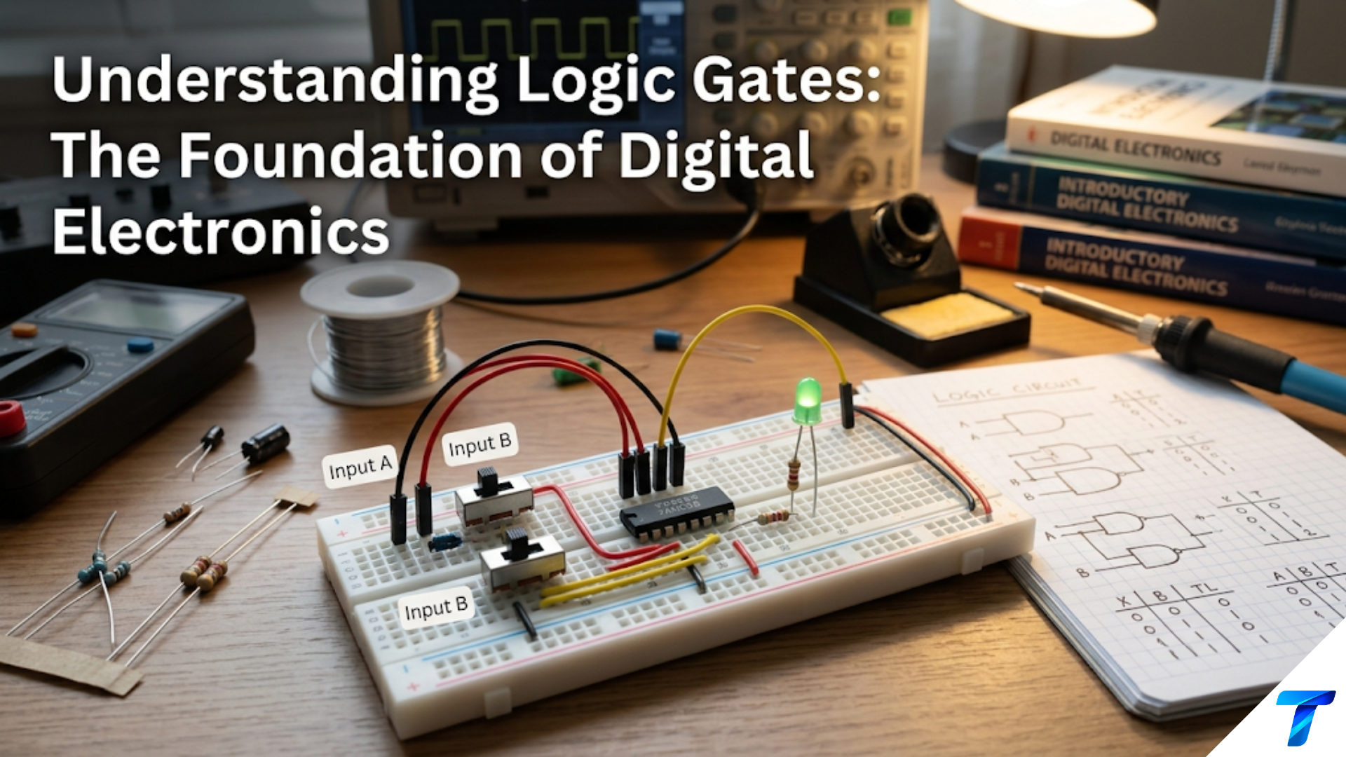
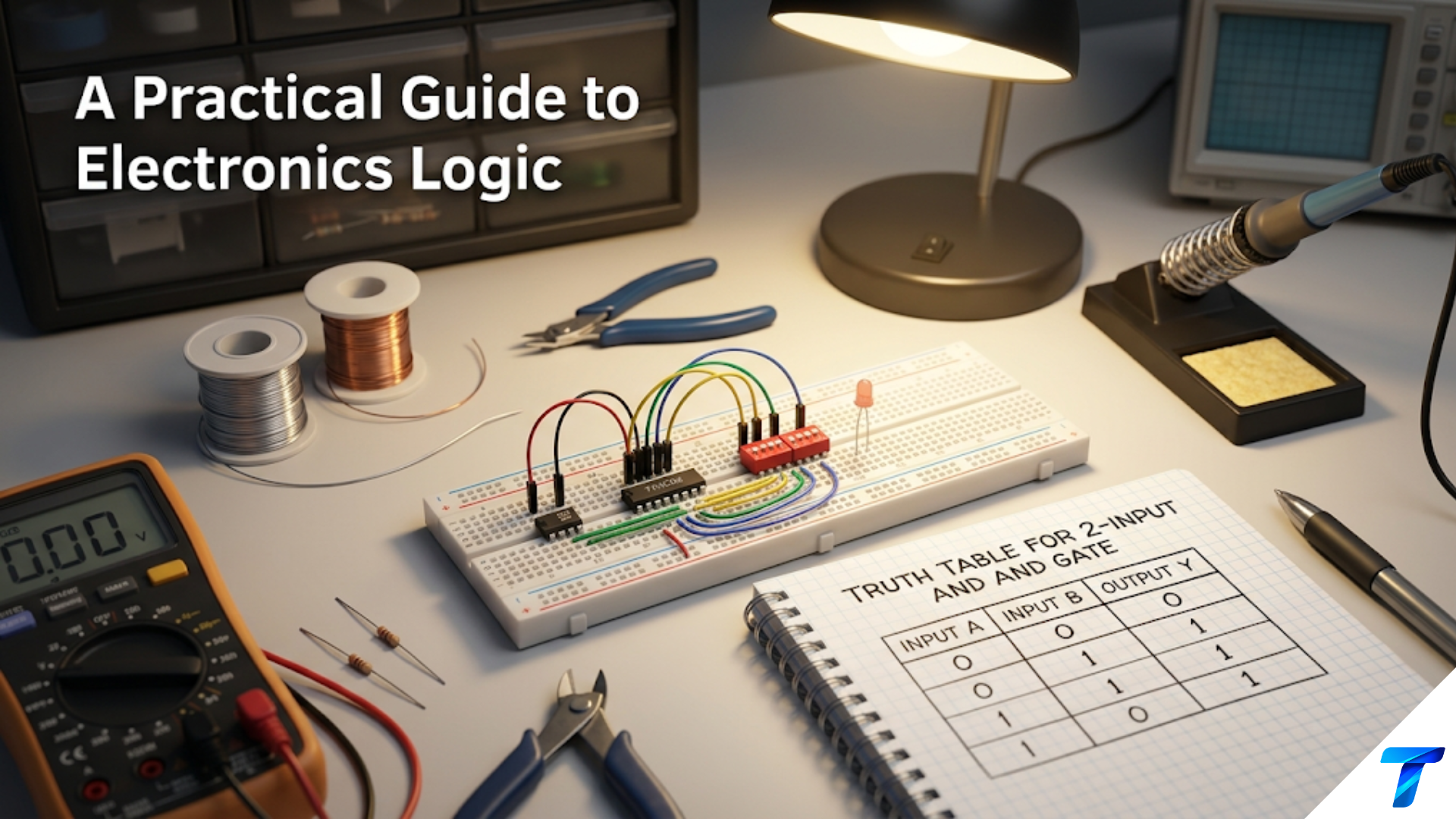
AND, OR, and NOT gates are the three fundamental building blocks of all digital logic. An AND gate outputs HIGH only when all its inputs are HIGH. An OR gate outputs HIGH when any input is HIGH. A NOT gate (inverter) outputs the opposite of its input. By combining these three gate types in different arrangements, any conceivable digital logic function — from a simple alarm circuit to a complete microprocessor — can be constructed, making them the universal vocabulary of digital electronics.
Introduction: The Grammar of Digital Logic
Every digital system — from a smartphone to a satellite — makes decisions by evaluating conditions. Is the temperature too high? Are both sensors active? Has either button been pressed? Is the password correct? At the silicon level, every one of these decisions ultimately reduces to combinations of three elemental operations: AND (both conditions true), OR (either condition true), and NOT (opposite of a condition).
These three operations are not arbitrary choices. In 1854, mathematician George Boole proved that all logical reasoning can be expressed using just these three operations — creating Boolean algebra, the mathematical foundation of modern computing. Almost a century later, Claude Shannon showed that Boolean algebra maps perfectly onto electrical circuits using switches: AND corresponds to switches in series, OR to switches in parallel, and NOT to a switch that inverts. When transistors replaced mechanical switches, the same logical structure remained but could now operate at billions of operations per second.
Understanding AND, OR, and NOT gates means understanding the fundamental grammar that all digital electronics speaks. Unlike analog circuits where continuous voltages carry information, digital logic circuits work with just two states: HIGH (logic 1, representing TRUE) and LOW (logic 0, representing FALSE). Every gate takes one or more binary inputs and produces a single binary output according to a fixed rule. Connect gates together, and those rules combine to implement any logic you can specify.
This article builds practical, hands-on knowledge of AND, OR, and NOT gates: what they do mathematically, how they are implemented in real integrated circuit packages, how to read and draw their schematic symbols, how to verify their behavior with truth tables, how to combine them into useful circuits, and how to design five complete working circuits from scratch using nothing but these three gate types. By the end, you will have the tools to translate any logical decision-making requirement into a working digital circuit.
The NOT Gate: The Simplest Logic Element
What a NOT Gate Does
The NOT gate — also called an inverter — is the simplest logic gate: one input, one output, and a single rule: the output is always the opposite of the input.
| Input A | Output Q |
|---|---|
| 0 | 1 |
| 1 | 0 |
If A is LOW, Q is HIGH. If A is HIGH, Q is LOW. The NOT gate simply flips the logic state.
Boolean Expression
The NOT operation is written with a bar (overline) above the variable, or with an apostrophe, or with the word NOT:
Q = Ā   (A-bar notation)
Q = A'  (apostrophe notation)
Q = NOT ARead as “Q equals NOT A” or “Q equals A-bar.”
Schematic Symbol
The NOT gate symbol is a triangle (representing a buffer/amplifier) with a small circle (bubble) at the output. The bubble is the universal symbol for inversion in digital electronics — you will see this bubble appear on many other gates and devices to indicate active-low or inverted signals.
    ___
A --|   >o-- Q
---The triangle points toward the output. The circle at the tip of the triangle indicates inversion.
Physical Implementation
At the transistor level, the simplest NOT gate is a single MOSFET with a pull-up resistor:
- When input A is HIGH (≥ V_IH): MOSFET conducts, output is pulled LOW through MOSFET to GND
- When input A is LOW (≤ V_IL): MOSFET is off, output is pulled HIGH through pull-up resistor to V_CC
This is an NMOS inverter — the foundation of all modern CMOS logic. Real CMOS inverters use a complementary PMOS pull-up and NMOS pull-down (no resistor needed), giving near-perfect rail-to-rail output swing and very low static power consumption.
Practical IC: 74HC04 Hex Inverter
The 74HC04 is the standard NOT gate IC in the 74HC (High-speed CMOS) logic family:
- Contains six independent inverters in a 14-pin DIP or SOIC package
- Supply: 2V to 6V (typically 5V or 3.3V)
- Output: totem-pole, rail-to-rail compatible
- Propagation delay: ~7ns at 5V
- Pin configuration: Each inverter uses one input pin and one output pin; pins 7 (GND) and 14 (VCC) are shared power rails
Pin assignments: 1A→1Y, 2A→2Y, 3A→3Y (left side); 4A→4Y, 5A→5Y, 6A→6Y (right side), with VCC on pin 14 and GND on pin 7.
Applications of the NOT Gate
Signal inversion: Converting active-high logic to active-low for devices that require it.
Buffer/driver (non-inverting): Two NOT gates in series produce a non-inverting buffer with the drive strength of a logic gate — useful for buffering weak signals or driving higher capacitance loads.
Oscillator (ring oscillator): Three (or any odd number of) NOT gates connected in a ring (output of gate 3 → input of gate 1) form an oscillator. Each gate inverts and delays, and the odd number of inversions means no stable state exists — the output continuously toggles. Frequency ≈ 1/(2 × N × t_pd) where N is the number of gates and t_pd is the propagation delay per gate. Not used for precision timing but useful for test circuits.
Debouncing with RC: A NOT gate with an RC input network forms a simple switch debouncer — the RC slows the input transition, and the Schmitt trigger characteristic of some NOT gates (74HC14) cleans up the edge.
The AND Gate: Logic Multiplication
What an AND Gate Does
The AND gate implements logical multiplication. Its output is HIGH only when ALL inputs are HIGH simultaneously. If any single input is LOW, the output is LOW.
Two-input AND gate truth table:
| Input A | Input B | Output Q |
|---|---|---|
| 0 | 0 | 0 |
| 0 | 1 | 0 |
| 1 | 0 | 0 |
| 1 | 1 | 1 |
The output is HIGH in exactly one row — when both A AND B are HIGH. For a 3-input AND gate, the output is HIGH only when A AND B AND C are all HIGH (one row out of eight). For an N-input AND gate, only 1 of 2^N input combinations produces a HIGH output.
Boolean Expression
The AND operation is written with a dot (·) or simply by juxtaposition (like multiplication):
Q = A · B   (dot notation)
Q = AB      (implicit notation)
Q = A AND BRead as “Q equals A AND B.”
Key Boolean identities for AND:
A · 0 = 0       (anything AND 0 = 0 — zero dominates)
A · 1 = A       (anything AND 1 = itself — one is neutral)
A · A = A       (idempotent law)
A · Ā = 0       (complementation law — A AND NOT-A = always 0)
A · B = B · A (commutative law)Schematic Symbol
The AND gate symbol has a flat input side and a curved (D-shaped) output side:
     ____
A --|    \
    |     )-- Q
B --|____/
The distinctive D-shaped curve on the output side identifies the AND gate. Three-input AND gates simply have three input lines entering the flat side.
Thinking About AND Gates
The AND gate asks: “Are all conditions simultaneously true?”
Physical analogy — series switches: Two switches in series (both must be closed for current to flow) implement AND logic. A deadman switch system (machine runs only when both operator presence switch AND safety guard switch are active) uses AND logic.
Real examples:
- A safety interlock: Motor runs only when POWER_ON AND DOOR_CLOSED AND OPERATOR_PRESENT
- A voting circuit: Majority vote requires at least 2 of 3 inputs HIGH — uses combinations of AND gates
- Address decoding in microprocessors: A specific memory address is selected only when all address lines match a specific pattern — AND of all required conditions
Practical ICs: 74HC08 and 74HC21
74HC08 — Quad 2-Input AND Gate:
- Four independent 2-input AND gates
- 14-pin DIP or SOIC
- Supply: 2V–6V
- Propagation delay: ~7ns at 5V
- Pin layout: 1A,1B→1Y; 2A,2B→2Y; 3A,3B→3Y; 4A,4B→4Y; VCC pin 14, GND pin 7
74HC21 — Dual 4-Input AND Gate:
- Two independent 4-input AND gates
- Useful when all four conditions must be true simultaneously
- 14-pin DIP
74HC11 — Triple 3-Input AND Gate:
- Three independent 3-input AND gates
The OR Gate: Logic Addition
What an OR Gate Does
The OR gate implements logical addition. Its output is HIGH when ANY input is HIGH — or when multiple inputs are simultaneously HIGH. The output is LOW only when ALL inputs are simultaneously LOW.
Two-input OR gate truth table:
| Input A | Input B | Output Q |
|---|---|---|
| 0 | 0 | 0 |
| 0 | 1 | 1 |
| 1 | 0 | 1 |
| 1 | 1 | 1 |
The output is LOW in exactly one row — when both A and B are LOW. For an N-input OR gate, only 1 of 2^N input combinations produces a LOW output (all inputs LOW).
Boolean Expression
The OR operation is written with a plus sign (+):
Q = A + B
Q = A OR BRead as “Q equals A OR B.” Note: the + sign in Boolean algebra means OR, not arithmetic addition. In Boolean algebra, 1 + 1 = 1 (not 2), because the output is HIGH regardless of how many inputs are HIGH.
Key Boolean identities for OR:
A + 0 = A       (zero is neutral for OR)
A + 1 = 1       (one dominates OR — anything OR 1 = 1)
A + A = A       (idempotent law)
A + Ā = 1       (complementation law — A OR NOT-A = always 1)
A + B = B + A (commutative law)Schematic Symbol
The OR gate symbol has a curved input side (concave) and a pointed output:
    ___
A --\   \
     )    >-- Q
B --/___/
The curved input side (concave arc on the back) and pointed output tip distinguish the OR gate from the AND gate’s flat input / curved output.
Thinking About OR Gates
The OR gate asks: “Is ANY condition true?”
Physical analogy — parallel switches: Two switches in parallel (either can be closed for current to flow) implement OR logic. Any light switch connected in parallel with another implements OR.
Real examples:
- An alarm system: ALARM = DOOR_OPEN OR WINDOW_OPEN OR MOTION_DETECTED
- An interrupt system: INTERRUPT_REQUEST = TIMER_OVERFLOW OR UART_DATA_READY OR BUTTON_PRESSED
- Error detection: ERROR = OVERVOLTAGE OR OVERCURRENT OR OVERTEMPERATURE
- Fault indication: Any one of multiple fault conditions triggers a warning LED
Practical ICs: 74HC32 and 74HC4075
74HC32 — Quad 2-Input OR Gate:
- Four independent 2-input OR gates
- 14-pin DIP or SOIC
- The most common OR gate IC
- Supply: 2V–6V, propagation delay ~7ns at 5V
74HC4075 — Triple 3-Input OR Gate:
- Three independent 3-input OR gates
Logic Levels and Electrical Specifications
Before building circuits, you need to understand what HIGH and LOW mean electrically and how to connect gates reliably.
Voltage Levels in 74HC Logic (5V Supply)
| Parameter | Symbol | Min | Typ | Max | Meaning |
|---|---|---|---|---|---|
| HIGH output | V_OH | 4.4V | 5.0V | — | Gate output guaranteed above this |
| LOW output | V_OL | — | 0V | 0.1V | Gate output guaranteed below this |
| HIGH input threshold | V_IH | 3.5V | — | — | Input must be above this for HIGH |
| LOW input threshold | V_IL | — | — | 1.0V | Input must be below this for LOW |
| Undefined region | — | 1.0V | — | 3.5V | Avoid inputs in this range |
The gap between V_OH (minimum 4.4V) and V_IH (minimum 3.5V) is the HIGH noise margin: 4.4V − 3.5V = 0.9V. Any noise up to 0.9V on a HIGH signal is rejected.
The gap between V_IL (maximum 1.0V) and V_OL (maximum 0.1V) is the LOW noise margin: 1.0V − 0.1V = 0.9V. This robust noise margin is why CMOS logic is inherently noise-resistant.
3.3V Logic (74LVC and 74ALVC Families)
For 3.3V microcontrollers (STM32, ESP32, Raspberry Pi), use the 74LVC family:
- Supply: 1.65V–3.6V
- V_IH: 2.0V, V_IL: 0.8V (at 3.3V supply)
- 5V input tolerant for many 74LVC devices — can accept 5V inputs while operating from 3.3V supply
- Same pinout as 74HC for drop-in compatibility
Fan-Out: How Many Inputs Can One Gate Drive?
Fan-out is the maximum number of same-family gate inputs that one gate output can reliably drive. For 74HC:
- Each output sources/sinks up to 25mA at the specified output voltage levels
- Each input draws < 1µA (CMOS input)
- Fan-out: 25mA / 1µA = 25,000 — effectively unlimited within a PCB
- Fan-out matters primarily when driving LEDs, transistors, or other non-CMOS loads
Unused Inputs: Never Leave Them Floating
Floating (unconnected) CMOS inputs are extremely dangerous — they pick up noise and settle to an undefined voltage in the transition region, causing excessive power consumption, erratic behavior, and potential latchup.
Rule: Every unused gate input must be tied to a defined logic level:
- Tie unused AND gate inputs to HIGH (V_CC through 10kΩ pull-up or directly) — HIGH is neutral for AND
- Tie unused OR gate inputs to LOW (GND directly or through pull-down) — LOW is neutral for OR
- Tie unused NOT gate inputs to either level — but avoid leaving them open
If an entire gate within an IC is unused:
- Tie its inputs to GND (for AND/NOT) or VCC (for OR) — safe and prevents oscillation
- Do NOT leave inputs open
Combining Gates: From Simple Logic to Complex Functions
The real power of logic gates emerges when they are combined. Any Boolean expression can be directly implemented as a gate network by following the expression’s structure.
Boolean Expression to Gate Circuit
Example: Implement Q = A·B + C (AND then OR)
Step 1: Identify operations in order of precedence. AND has higher precedence than OR (like multiplication before addition), so A·B is computed first.
Step 2: Draw gates following the expression:
- Gate 1 (AND): inputs A and B, output = A·B (intermediate signal)
- Gate 2 (OR): inputs are A·B (from Gate 1) and C, output = Q
Two gates total. This circuit outputs HIGH if (A AND B) OR C is true.
Example: Implement Q = (A + B) · C (OR then AND)
- Gate 1 (OR): inputs A and B, output = A+B
- Gate 2 (AND): inputs A+B and C, output = Q
Same two-gate structure, different gate types. Output HIGH only if (A OR B) AND C.
Example: Implement Q = Ā · B + A · B̄ (XOR using AND, OR, NOT)
This is the Exclusive-OR function (output HIGH when inputs differ):
- Gate 1 (NOT): input A, output = Ā
- Gate 2 (NOT): input B, output = B̄
- Gate 3 (AND): inputs Ā and B, output = Ā·B
- Gate 4 (AND): inputs A and B̄, output = A·B̄
- Gate 5 (OR): inputs Ā·B and A·B̄, output = Q
Five gates using only AND, OR, and NOT. This demonstrates the universality of these three gates — any logic function, including XOR, can be built from them.
De Morgan’s Laws: Essential for Gate Simplification
De Morgan’s laws are the most important identities for simplifying logic circuits:
Law 1: NOT(A AND B) = (NOT A) OR (NOT B)
-(A·B) = Ā + B̄Law 2: NOT(A OR B) = (NOT A) AND (NOT B)
-(A+B) = Ā · B̄How to remember: “Break the bar, change the sign” — when you remove an inversion from a multi-variable expression, you change AND to OR or OR to AND.
Practical application: De Morgan’s laws let you convert between AND-based and OR-based implementations. This is crucial for optimization — sometimes one implementation uses fewer gates than another. Also, since NAND and NOR gates are more available and more efficient than AND/OR in CMOS technology, De Morgan’s laws help you convert AND/OR expressions to NAND/NOR implementations.
Example: Implement (A + B)’ (NOT of A OR B) using AND and NOT gates (no OR gate available):
By De Morgan’s Law 2: (A + B)’ = A’ · B’
- Gate 1 (NOT): input A, output = A’
- Gate 2 (NOT): input B, output = B’
- Gate 3 (AND): inputs A’ and B’, output = (A+B)’
Equivalent result using only NOT and AND — no OR gate needed.
Multi-Level Logic
Complex logic functions often require multiple levels of gates (the output of one level feeds the input of the next). Each level adds propagation delay — the total delay equals the sum of delays through each gate in the critical path.
For a circuit with 4 levels of 74HC gates (each 7ns delay):
Total propagation delay = 4 × 7ns = 28ns
Maximum clock frequency ≤ 1 / (28ns) ≈ 35MHz (with no margin)In practice, timing margins of 2–3× are required for reliable operation, limiting this circuit to about 10–15MHz. For higher-speed designs, minimizing gate levels is critical.
The Decoupling Capacitor: Essential for Every Logic IC
Before building any gate circuit, you must understand decoupling capacitors. This is not optional — without decoupling, digital circuits produce massive EMI, cause voltage glitches that corrupt logic states, and often simply malfunction.
Why Logic Gates Need Decoupling
When a logic gate switches states, its output transistors briefly conduct simultaneously (both pull-up and pull-down on during the transition), drawing a large transient current spike from the supply. This spike flows through the supply trace inductance, causing a voltage glitch on VCC:
ΔV = L_trace × dI/dtFor L = 10nH and dI/dt = 50mA / 2ns:
ΔV = 10×10⁻⁹ × 50×10⁻³ / 2×10⁻⁹ = 250mVA 250mV glitch on a 5V supply is 5% — enough to corrupt adjacent logic. With multiple gates switching simultaneously (common in digital circuits), glitches multiply.
Solution: Place a 100nF ceramic capacitor between VCC and GND as close as possible (within 3mm) to every logic IC’s power pins. This capacitor supplies the instantaneous switching current locally, preventing the current from flowing through the long supply trace and causing glitches.
Rule: One 100nF ceramic capacitor per IC package, placed within 3mm of the VCC pin. For boards with many ICs, also add a 10µF electrolytic bulk capacitor near the supply connector.
Complete Design Examples
Design Example 1: Three-Input Majority Voter
Application: A safety system with three independent sensors (A, B, C). Trigger an alarm if any two or more sensors detect a fault. A single sensor false alarm should NOT trigger — this prevents nuisance alarms from single-sensor failures.
Logic requirement: Output HIGH when 2 or more of 3 inputs are HIGH.
This is a majority vote function. Let’s derive the Boolean expression from the truth table:
| A | B | C | Q | Condition |
|---|---|---|---|---|
| 0 | 0 | 0 | 0 | None |
| 0 | 0 | 1 | 0 | Only C |
| 0 | 1 | 0 | 0 | Only B |
| 0 | 1 | 1 | 1 | B and C |
| 1 | 0 | 0 | 0 | Only A |
| 1 | 0 | 1 | 1 | A and C |
| 1 | 1 | 0 | 1 | A and B |
| 1 | 1 | 1 | 1 | All three |
The output is HIGH in four rows. Write the Boolean expression as the OR of minterms (Sum of Products):
Q = (Ā·B·C) + (A·B̄·C) + (A·B·C̄) + (A·B·C)Simplification: Factor common terms:
- From rows 4 and 8: B·C appears in both → B·C(Ā + A) = B·C·1 = B·C
- From rows 6 and 8: A·C appears in both → A·C(B̄ + B) = A·C
- From rows 7 and 8: A·B appears in both → A·B(C̄ + C) = A·B
Simplified expression:
Q = A·B + A·C + B·CGate implementation:
Using three 2-input AND gates and one 3-input OR gate:
- Gate 1 (AND): inputs A, B → output = A·B
- Gate 2 (AND): inputs A, C → output = A·C
- Gate 3 (AND): inputs B, C → output = B·C
- Gate 4 (OR, 3-input): inputs A·B, A·C, B·C → output Q
ICs required:
- Half of a 74HC08 (Quad 2-input AND) — uses 3 of 4 AND gates
- One 74HC4075 (Triple 3-input OR) — uses 1 of 3 OR gates
Alternative with 2-input OR gates (74HC32): Replace the 3-input OR with two 2-input ORs:
- Gate 4 (OR): inputs A·B and A·C → output = A·B + A·C
- Gate 5 (OR): inputs (A·B + A·C) and B·C → output Q
Total: 3 AND gates + 2 OR gates = 5 gates from two ICs (74HC08 + 74HC32).
Verification (partial): Test with A=1, B=1, C=0:
A·B = 1·1 = 1
A·C = 1·0 = 0
B·C = 1·0 = 0
Q = 1 + 0 + 0 = 1 ✓ (correct — two sensors active)Test with A=1, B=0, C=0:
A·B = 0, A·C = 0, B·C = 0 → Q = 0 ✓ (correct — only one sensor)Design Example 2: Four-Input Priority Alarm with Enable
Application: An industrial monitoring system with four alarm inputs (A, B, C, D) and a system ENABLE line. The alarm output should activate if any alarm input is active AND the system is enabled. Additionally, alarms A and B are high-priority and should latch the system — not just activate the alarm. For this design, implement just the alarm activation logic (latching is handled by flip-flops in a later article).
Logic requirement:
ALARM = ENABLE · (A + B + C + D)Gate implementation:
Option 1: OR all inputs first, then AND with ENABLE:
- Gate 1 (OR): inputs A, B → output = A+B
- Gate 2 (OR): inputs C, D → output = C+D
- Gate 3 (OR): inputs (A+B) and (C+D) → output = A+B+C+D
- Gate 4 (AND): inputs ENABLE and (A+B+C+D) → output = ALARM
Total: 3 OR gates + 1 AND gate (one 74HC32 for the three OR gates + half of a 74HC08).
Option 2: AND each input with ENABLE first, then OR all:
- Gates 1–4 (AND): each input ANDed with ENABLE
- A·ENABLE, B·ENABLE, C·ENABLE, D·ENABLE
- Gate 5 (OR): A·ENABLE + B·ENABLE
- Gate 6 (OR): C·ENABLE + D·ENABLE
- Gate 7 (OR): output of Gate 5 + output of Gate 6
Total: 4 AND + 3 OR = 7 gates (two full ICs)
Option 1 uses fewer gates. Both produce identical outputs — Boolean algebra confirms they are equivalent:
ENABLE · (A+B+C+D) = A·ENABLE + B·ENABLE + C·ENABLE + D·ENABLE(Distribution law — AND distributes over OR)
ICs required (Option 1): 74HC32 (Quad 2-input OR, uses 3 gates) + 74HC08 (uses 1 gate). Plus one gate from 74HC32 is spare — tie its inputs to GND.
Adding LED output driver:
Logic gate outputs can directly drive LEDs with a series resistor, but the LED current (typically 10–20mA) should be sourced/sunk by the gate output. 74HC gates sink up to 25mA — adequate for one LED.
ALARM output → 470Ω → LED anode → LED cathode → GNDLED current: (5V − 2V_f) / 470Ω = (5 − 2) / 470 ≈ 6.4mA — safe for both the gate and LED.
Adding a buzzer:
A piezo buzzer (high-impedance) can be driven directly. A magnetic buzzer (lower impedance, typically 100Ω–200Ω) draws too much current for a gate output. Drive a magnetic buzzer through a transistor:
ALARM → 1kΩ base resistor → NPN transistor base
NPN collector → buzzer → VCC
NPN emitter → GND
Flyback diode across buzzer (buzzer has inductance)Design Example 3: Combinational Lock (3-Bit Code Detector)
Application: A simple 3-bit combination lock. Eight possible input combinations (DIP switches or keypad). Output HIGH only for the correct combination: A=1, B=0, C=1 (binary 101 = decimal 5). Drive a relay to unlock a door.
Logic requirement: Output HIGH only when A=1 AND B=0 AND C=1.
To detect B=0, we need to invert B first (we want B̄, not B):
Q = A · B̄ · CGate implementation:
- Gate 1 (NOT): input B, output = B̄
- Gate 2 (AND, 3-input): inputs A, B̄, C → output Q
ICs: One 74HC04 (for the NOT gate, 5 gates spare) + one 74HC11 (Triple 3-input AND, uses 1 gate, 2 spare).
Verification:
| A | B | C | B̄ | A·B̄·C = Q | Correct? |
|---|---|---|---|---|---|
| 1 | 0 | 1 | 1 | 1·1·1 = 1 | ✓ Unlocks |
| 1 | 1 | 1 | 0 | 1·0·1 = 0 | ✓ Wrong code |
| 0 | 0 | 1 | 1 | 0·1·1 = 0 | ✓ Wrong code |
| 1 | 0 | 0 | 1 | 1·1·0 = 0 | ✓ Wrong code |
Only the combination A=1, B=0, C=1 produces a HIGH output. All other combinations produce LOW.
Extending to more bits:
For a 4-bit code (A=1, B=0, C=1, D=1):
Q = A · B̄ · C · DGate 1 (NOT): B → B̄ Gate 2 (AND, 4-input from 74HC21): A, B̄, C, D → Q
For an 8-bit code, split into two 4-bit groups, AND each group, then AND the two results — three AND gates total.
Relay driver:
The logic gate output drives the relay through a transistor (relay coils draw 50–200mA, far exceeding gate output capability):
Q → 4.7kΩ → NPN base (BC547)
NPN collector → relay coil → V_relay_supply
NPN emitter → GND
1N4007 flyback diode across relay coil (essential!)
Relay normally-open contact → door lock mechanismWhen Q = HIGH: transistor saturates, relay coil energizes, contact closes, door unlocks. When Q = LOW: transistor off, relay de-energizes, contact opens, door locks.
Design Example 4: Automatic Lighting Controller
Application: Garden path lights that turn on automatically when it is dark AND (either someone is present OR it is within programmed hours). Three inputs:
- DARK: HIGH when ambient light is below threshold (from LDR + comparator circuit)
- MOTION: HIGH when PIR motion sensor detects presence
- TIMER: HIGH when a timer circuit indicates scheduled on-hours
Logic requirement:
LIGHTS_ON = DARK · (MOTION + TIMER)Gate implementation:
- Gate 1 (OR): inputs MOTION, TIMER → output = MOTION + TIMER
- Gate 2 (AND): inputs DARK, (MOTION + TIMER) → output = LIGHTS_ON
Total: 1 OR gate + 1 AND gate. These two gates come from one 74HC08 (AND) and one 74HC32 (OR), with 3 AND gates and 3 OR gates spare.
Sensor interfacing:
The DARK signal comes from an LDR (light-dependent resistor) voltage divider feeding a comparator (like the LM393) with hysteresis. As discussed in previous articles, the comparator outputs a digital HIGH/LOW signal compatible with 74HC input levels.
The MOTION signal comes from a PIR (passive infrared) sensor module that outputs a 3.3V or 5V HIGH when motion is detected — directly compatible with 74HC inputs (with a pull-down resistor if the PIR output is open-drain).
The TIMER signal comes from a 555 timer circuit in astable mode, or from a microcontroller GPIO pin, or from a dedicated timer IC.
Output stage (driving a solid-state relay for 230V lighting):
LIGHTS_ON → 470Ω → LED of solid-state relay (SSR) input SSR output terminals connect to 230V AC lighting circuit
The SSR provides complete galvanic isolation between the 5V logic circuit and the mains voltage. Never connect logic circuits directly to mains — always use an SSR or relay for isolation.
Adding a manual override:
Add an OVERRIDE switch input. When OVERRIDE = HIGH (manual on), lights should be on regardless of other conditions:
LIGHTS_ON = DARK · (MOTION + TIMER) + OVERRIDEAdd Gate 3 (OR): inputs = output_of_Gate_2 and OVERRIDE → final LIGHTS_ON output.
Three gates total — still fits within the spare gates of the same two ICs.
Design Example 5: Binary Address Decoder (2-to-4 Line)
Application: A microcontroller has 2 address bits (A0, A1) selecting one of four peripheral devices. Exactly one device enable signal should be HIGH for each address combination. This is a 2-to-4 line decoder — fundamental in memory and peripheral interfacing.
Truth table:
| A1 | A0 | Y0 | Y1 | Y2 | Y3 | Selected |
|---|---|---|---|---|---|---|
| 0 | 0 | 1 | 0 | 0 | 0 | Device 0 |
| 0 | 1 | 0 | 1 | 0 | 0 | Device 1 |
| 1 | 0 | 0 | 0 | 1 | 0 | Device 2 |
| 1 | 1 | 0 | 0 | 0 | 1 | Device 3 |
Boolean expressions for each output:
Y0 = Ā1 · Ā0   (neither address bit HIGH)
Y1 = Ā1 · A0   (only A0 HIGH)
Y2 = A1 · Ā0   (only A1 HIGH)
Y3 = A1 · A0 (both address bits HIGH)Gate implementation:
- Gate 1 (NOT): input A0 → Ā0
- Gate 2 (NOT): input A1 → Ā1
- Gate 3 (AND): inputs Ā1, Ā0 → Y0
- Gate 4 (AND): inputs Ā1, A0 → Y1
- Gate 5 (AND): inputs A1, Ā0 → Y2
- Gate 6 (AND): inputs A1, A0 → Y3
Total: 2 NOT gates + 4 AND gates.
ICs: One 74HC04 (hex inverter, uses 2 of 6) + one 74HC08 (quad 2-input AND, uses all 4 gates exactly).
Verification:
Test with A1=1, A0=0 (should select Y2):
- Ā0 = NOT(0) = 1
- Ā1 = NOT(1) = 0
- Y0 = 0·1 = 0 ✓
- Y1 = 0·0 = 0 ✓
- Y2 = 1·1 = 1 ✓ (selected)
- Y3 = 1·0 = 0 ✓
Enable input (active-low chip select):
Professional decoder ICs include an active-low enable input (CS̄ — chip select bar). When CS̄ = LOW (enabled), the decoder works normally. When CS̄ = HIGH (disabled), all outputs are forced LOW.
Implement with additional AND gates:
- Each output AND’d with (NOT CS̄ = CS):
Y0 = Ā1·Ā0·CS
Y1 = Ā1·A0·CS
Y2 = A1·Ā0·CS
Y3 = A1·A0·CSThis requires 3-input AND gates (74HC11) instead of 2-input, adding one more IC. Real decoder ICs (74HC139, 74HC138) implement this function in a single package — but building it from basic gates demonstrates exactly how they work internally.
Practical note: The 74HC138 (3-to-8 line decoder) and 74HC139 (dual 2-to-4 line decoder) are standard ICs that implement exactly this function, optimized and tested. When building real systems, use these instead of discrete gate networks. But understanding the gate-level implementation is essential for comprehending how all decoders, multiplexers, and address logic works.
Timing Diagrams: Visualizing Gate Behavior Over Time
A timing diagram shows how logic signals change over time, revealing gate behavior during sequential input changes.
Reading a Timing Diagram
For the circuit Q = A·B (AND gate):
Time:   0   1   2   3   4   5   6   7   8
A:      0   0   1   1   0   1   1   0   0
B:      0   1   0   1   1   0   1   1   0

Q=A·B: 0 0 0 1 0 0 1 0 0Reading: Q is HIGH (time 3–4) when both A and B are HIGH simultaneously, and again at time 6–7. At all other times, at least one input is LOW so Q is LOW.
Propagation Delay in Timing Diagrams
Real gates do not switch instantaneously. The propagation delay (t_pd, typically 7ns for 74HC at 5V) appears as a slight horizontal offset between input change and output change:
Input A changes HIGH at t=100ns
Output Q changes HIGH at t=107ns (7ns propagation delay)For multi-level circuits, delays cascade:
Gate 1 (AND): output changes at t + 7ns
Gate 2 (OR):  output changes at t + 14ns (7ns + 7ns)
Gate 3 (NOT): output changes at t + 21nsThis cascaded delay sets the maximum operating frequency of the circuit and must be accounted for in all timing calculations.
Breadboard Construction Tips for Logic Gate Circuits
Power Supply Setup
- Connect VCC rail to 5V (for 74HC) — use a dedicated 5V regulator or laboratory supply
- Connect GND rail to ground
- Place 100µF electrolytic capacitor across power rails at the supply connection
- Each IC needs its own 100nF ceramic decoupling capacitor directly at its VCC and GND pins
Component Placement
- Place ICs across the center divide of the breadboard (DIP packages straddle the gap)
- Keep signal wires short — long wires act as antennas and pick up noise
- Color-code wires: red for VCC, black for GND, other colors for signals
- Label or mark which gate in an IC you are using
Input Switches
For manual logic inputs (testing):
- Connect a SPDT (single-pole double-throw) switch between VCC and GND
- Connect the switch wiper (center) to the gate input through a 1kΩ series resistor
- The 1kΩ resistor protects against accidental shorts if the switch briefly contacts both rails
- This gives a clean HIGH (close to VCC) or LOW (close to GND) with no floating states
Output Indication
For output monitoring:
- LED + 470Ω series resistor from output to GND for active-HIGH indication
- LED lights when output is HIGH (≥ 2V forward voltage + drop across 470Ω)
- Current: (5V − 2V) / 470Ω ≈ 6.4mA — safe for 74HC outputs and LEDs
Testing Procedure
- Check power supply voltage with multimeter before inserting ICs
- Insert ICs and add decoupling capacitors
- Connect all unused inputs to VCC or GND as appropriate
- Apply inputs systematically through all truth table combinations
- Verify output matches truth table for each combination
- If behavior is incorrect: check power, check pin numbers, check decoupling, check for floating inputs
Common Mistakes and How to Avoid Them
Mistake 1: Leaving inputs floating Any unconnected CMOS input floats to an indeterminate voltage. The output becomes unpredictable. Always tie unused inputs to VCC or GND.
Mistake 2: Wrong pin numbers The 74HC04 (NOT), 74HC08 (AND), and 74HC32 (OR) all have the same 14-pin package, but different internal arrangements. Always check the datasheet pinout — never assume from memory.
Mistake 3: Omitting decoupling capacitors The circuit may work most of the time but fails intermittently under noise or during fast switching. Add 100nF ceramic at every IC’s VCC pin.
Mistake 4: Mixing 5V and 3.3V logic without level shifting 74HC (5V) logic outputs (4.4V minimum) are too high for 3.3V device inputs (3.3V maximum). Use 74LVC (3.3V) logic and a level shifter at the interface, or use 5V-tolerant inputs.
Mistake 5: Driving LEDs or buzzers directly from a gate output without a current-limiting resistor A directly connected LED draws unlimited current (limited only by the LED’s forward resistance — very low). The gate output transistor burns out. Always use a series resistor: R = (V_OH − V_f) / I_LED, typically 330Ω–1kΩ.
Mistake 6: Confusing Boolean + (OR) with arithmetic + (addition) In Boolean algebra: 1 + 1 = 1 (not 2). This is OR, not addition. Similarly, 1 · 1 = 1 and 0 · 1 = 0 follow normal arithmetic rules for AND. The confusion arises because the same symbols (+, ·) are used for both.
Mistake 7: Incorrect De Morgan’s law application ̄(A·B) ≠ Ā · B̄ — this is the most common Boolean algebra error. Correctly: ̄(A·B) = Ā + B̄ (change AND to OR when distributing the bar). The sign must change when the bar is broken.
Summary
AND, OR, and NOT gates are the complete logical vocabulary of digital electronics. NOT inverts a signal (Q = Ā). AND outputs HIGH only when all inputs are HIGH (Q = A·B). OR outputs HIGH when any input is HIGH (Q = A+B). Every Boolean expression can be directly translated into a gate network, and any gate network can be analyzed using Boolean algebra.
Key Boolean identities — the domination laws (A·0=0, A+1=1), identity laws (A·1=A, A+0=A), idempotent law (A·A=A), and complementation (A·Ā=0, A+Ā=1) — simplify expressions before implementation. De Morgan’s laws (break the bar, change the sign) enable conversion between AND-based and OR-based implementations.
Practical implementation uses standard 74HC family ICs: 74HC04 (hex NOT), 74HC08 (quad 2-input AND), 74HC32 (quad 2-input OR), plus multi-input variants. Every IC requires a 100nF ceramic decoupling capacitor at its VCC pin, and every unused input must be tied to a defined logic level.
The five design examples — majority voter, priority alarm, combination lock, automatic lighting controller, and address decoder — show how these three gates combine to implement any real-world logic decision, from safety systems to microcontroller interfacing.