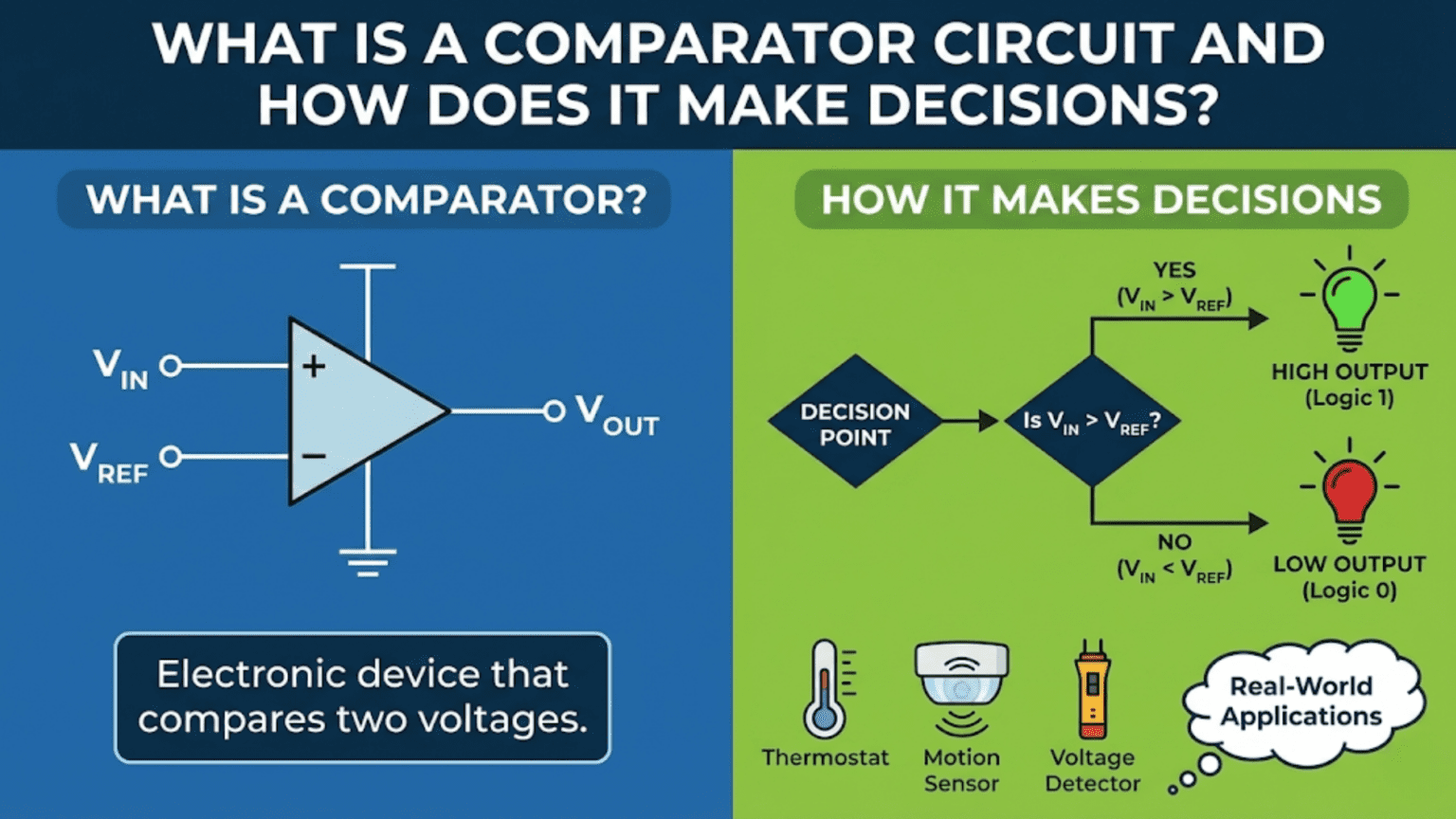
A comparator circuit is an electronic circuit that compares two input voltages and produces a digital output indicating which is larger output goes high when the non-inverting input exceeds the inverting input, and low when it does not. Comparators are used to detect when a signal crosses a threshold, convert analog signals to digital logic levels, and trigger actions in response to sensor readings, appearing in everything from battery monitors to temperature controllers and zero-crossing detectors.
Introduction: The Circuit That Answers a Single Question
Every decision in electronics ultimately reduces to a single binary question: is this voltage higher or lower than that voltage? Is the battery charged enough? Has the temperature crossed the alarm threshold? Is the signal above zero? Has the wheel spun fast enough? Did the light level drop below the setpoint?
These are threshold questions — and the circuit that answers them is the comparator.
Unlike the amplifier circuits covered in the previous articles, which use negative feedback to produce a proportional, linear output, the comparator operates very differently. It deliberately operates without stabilizing feedback, or with positive feedback that reinforces switching rather than moderating it. The result is not a proportional output but a binary one: the output snaps to one extreme (high) or the other (low) depending on which of the two inputs is larger. There is no middle ground.
This binary behavior makes the comparator the bridge between the analog world and the digital world. Temperature, pressure, light, voltage, current — these are all analog quantities that vary continuously. Decisions, triggers, alarms, and logic signals are binary. The comparator performs the conversion: when the analog sensor reading crosses a threshold, the comparator output changes state, triggering whatever digital action is required.
Comparators appear in virtually every electronic system. Your laptop’s battery management IC uses comparators to detect when the battery voltage drops below safe levels. Your washing machine’s water level sensor uses a comparator to signal when the tank is full. Your car’s fuel injection system uses comparators to time ignition signals. Switching power supplies use comparators in their pulse-width modulation control loops. Every analog-to-digital converter uses comparators at its core.
This article builds a complete understanding of comparator circuits from first principles: what makes a comparator different from a linear amplifier, how to build basic comparator circuits, how to set thresholds precisely, how to use hysteresis to prevent false triggering from noisy signals, what dedicated comparator ICs offer over op-amps, and how to design reliable comparator circuits for real applications.
What Makes a Comparator Different from a Linear Amplifier
The Open-Loop Distinction
The fundamental difference between a comparator and the amplifier circuits discussed in previous articles is feedback.
The inverting and non-inverting amplifiers use negative feedback — a portion of the output is fed back to the inverting input, opposing any change in output voltage and stabilizing the gain at a precise value determined by external resistors. This feedback keeps the op-amp operating in its linear region, where the output is a proportional amplification of the input difference.
A comparator operates open-loop — with no negative feedback path. Without feedback to stabilize the output, the op-amp’s enormous open-loop gain (100,000 to 1,000,000) takes even the tiniest input voltage difference and amplifies it to saturation. A difference of just 50µV at the input of a gain-200,000 op-amp would produce an ideal output of 10V — which clips at the supply rail. In practice, the output slams fully to one supply rail or the other based purely on which input is higher.
This is exactly what a comparator needs to do: make a sharp, decisive, digital-like output transition.
Linear Region vs. Saturation: A Visual Contrast
Consider an op-amp with open-loop gain A_OL = 200,000 operating from ±12V supply:
- If V+ − V− = +100µV: V_out = 200,000 × 100µV = 20V → clips at +12V (output HIGH)
- If V+ − V− = −100µV: V_out = 200,000 × (−100µV) = −20V → clips at −12V (output LOW)
- If V+ − V− = 0V exactly: V_out = 0V (the knife’s edge — unstable without feedback)
The transition from output LOW to output HIGH occurs over an input range of just ±60µV (12V / 200,000). For any practical signal with millivolt or larger variations, this transition is instantaneous — the output appears to switch instantly at the crossover point.
This is the comparator’s defining behavior: a sharp, decisive switch at the moment the two input voltages are equal, producing a digital-like output from analog inputs.
The Transfer Characteristic
The input-output relationship of a comparator is:
V_out = V_OH    when V+ > V−   (output high)
V_out = V_OL when V+ < V− (output low)Where V_OH is the output high voltage (near the positive supply) and V_OL is the output low voltage (near the negative supply or ground). The transition between these two states occurs at the crossover point V+ = V−.
For a single-threshold comparator with a fixed reference on V−:
V_out = V_OH    when V_in > V_ref   (input above threshold)
V_out = V_OL when V_in < V_ref (input below threshold)This creates a simple decision: is the input above or below the reference voltage?
The Basic Comparator Circuit
Circuit 1: Non-Inverting Comparator
Connect the signal to the non-inverting input (V+) and the reference voltage to the inverting input (V−):
- V_in → V+ (signal being compared)
- V_ref → V− (threshold reference voltage)
- V_out = pin 3 (comparison result)
- No feedback resistor
Behavior:
- When V_in > V_ref: V_out → V_OH (high — signal above threshold)
- When V_in < V_ref: V_out → V_OL (low — signal below threshold)
Output polarity matches the comparison intuitively: “signal above threshold” → output high.
Circuit 2: Inverting Comparator
Connect the signal to the inverting input (V−) and the reference to the non-inverting input (V+):
- V_ref → V+
- V_in → V−
Behavior:
- When V_in > V_ref: V_out → V_OL (low — signal above threshold → output low)
- When V_in < V_ref: V_out → V_OH (high — signal below threshold → output high)
Output polarity is inverted relative to the comparison: “signal above threshold” → output low. This is useful when the downstream logic requires an active-low signal or when you need to invert the decision logic.
Setting the Reference Voltage
The reference voltage V_ref determines the threshold at which the comparator switches. Three common methods:
Method 1: Fixed resistor voltage divider
Two resistors from VCC to GND create V_ref at their junction:
V_ref = VCC × R2 / (R1 + R2)Where R1 is the top resistor (VCC to junction) and R2 is the bottom resistor (junction to GND).
Example: VCC = 5V, threshold at 2.5V (50%): R1 = R2 = 10kΩ → V_ref = 5V × 10k/(10k+10k) = 2.5V
Example: VCC = 9V, threshold at 3V (1/3 supply): R1 = 20kΩ, R2 = 10kΩ → V_ref = 9V × 10k/30k = 3V
Use 1% tolerance resistors for accurate threshold setting. The voltage divider should have low enough impedance that load current from the comparator’s input doesn’t shift V_ref — keep R1 + R2 below 100kΩ for most op-amp comparators (which draw some input bias current).
Method 2: Potentiometer (adjustable threshold)
Replace the fixed resistor divider with a potentiometer. Rotating the pot adjusts the threshold continuously. Use a multi-turn cermet potentiometer for stable, precise adjustment in calibration circuits.
Method 3: Zener diode reference
For a precise, supply-independent threshold, a Zener diode in series with a resistor from VCC creates a stable reference voltage equal to the Zener’s breakdown voltage. A 3.3V Zener gives a 3.3V threshold regardless of VCC variation (as long as VCC > 3.3V + enough voltage drop across the series resistor).
R_series = (VCC − V_zener) / I_zenerFor stable Zener operation, keep I_zener between 5mA and 20mA for standard 1/2W Zener diodes.
Window Comparator: Detecting a Voltage Range
A single comparator detects whether a voltage is above or below one threshold. But sometimes you need to know whether a voltage is within a range — between a lower and upper bound. A window comparator answers this question using two comparators.
Window Comparator Circuit
Comparator 1 (lower bound):
- V_ref_low → V− (lower threshold)
- V_in → V+
- Output HIGH when V_in > V_ref_low
Comparator 2 (upper bound):
- V_in → V− (or V_ref_high → V+, with V_in → V+; depending on desired output logic)
- V_ref_high → V+ (upper threshold)
- Output HIGH when V_in < V_ref_high (inverting comparator — output HIGH when below upper bound)
Logic combination: AND the two outputs. The AND gate output is HIGH only when V_in > V_ref_low AND V_in < V_ref_high — that is, when V_in is within the window.
Many dedicated comparator ICs (like the LM339 quad comparator) have open-collector outputs that can be wire-ANDed by simply connecting them together with a pull-up resistor — no separate AND gate needed. The combined output is high only when all connected outputs are high simultaneously.
Applications:
- Battery charge monitoring (detecting voltage between fully discharged and fully charged thresholds)
- Tolerance testing (is the measured value within acceptable limits?)
- Speed monitoring (is the measured frequency within the allowed range?)
- ADC flash conversion (a bank of window comparators determines which voltage range the input falls into)
The Problem with Simple Comparators: Noise and Chatter
A simple open-loop comparator works perfectly in an ideal world. In the real world, it has a critical weakness: chatter near the threshold.
What Is Chatter?
Real signals are never perfectly clean. They contain noise — random voltage fluctuations from thermal agitation, electromagnetic interference, power supply ripple, and other sources. When the signal is close to the threshold, the noise causes the signal to repeatedly cross the threshold back and forth many times per second.
Each threshold crossing causes the comparator to switch — potentially dozens or hundreds of times per millisecond when the signal hovers near the threshold. The output becomes a rapid, chaotic burst of pulses rather than a clean single transition.
This chatter causes serious problems downstream:
- A digital counter connected to the comparator output counts hundreds of spurious pulses
- A relay driver chatters the relay on and off rapidly, damaging contacts
- A microcontroller interrupt fires dozens of times from what should be a single event
- Audio amplifiers driven from the comparator output produce a buzzing noise
- Motor controllers cycle on and off rapidly, causing motor heating and mechanical stress
Visualizing the Chatter Problem
Imagine a temperature sensor signal slowly rising toward a 30°C threshold:
- Temperature = 29.8°C: output LOW (below threshold)
- Temperature = 30.1°C + 0.3°C noise: output briefly goes HIGH then LOW (noise spike)
- Temperature = 30.0°C: at threshold — noise of ±0.2°C causes repeated switching
- Temperature = 30.2°C: output HIGH (above threshold)
During the period when temperature ≈ threshold, the output chatters hundreds of times from the noise alone. A clean single transition is impossible with a single-threshold comparator when the signal has any noise.
The solution is hysteresis.
Hysteresis: The Key to Reliable Comparator Design
Hysteresis transforms a chattering comparator into a clean, decisive switching circuit. It works by making the threshold different depending on which direction the input is moving — creating a dead band between the upper and lower switching thresholds.
What Hysteresis Does
Instead of one threshold, a comparator with hysteresis has two:
- Upper threshold (V_TH+): The input must rise above this level to switch the output from LOW to HIGH
- Lower threshold (V_TH−): The input must fall below this level to switch the output from HIGH to LOW
The difference between these thresholds is the hysteresis voltage (also called the dead band):
V_hys = V_TH+ − V_TH−For the comparator to chatter, the noise would have to exceed V_hys in amplitude — moving the signal from below V_TH− to above V_TH+ in a single noise excursion. By setting V_hys larger than the peak noise amplitude, chatter is prevented entirely.
The trade-off: A wider hysteresis band prevents noise-induced chatter but reduces the circuit’s ability to detect small signals near the threshold. The signal must change by at least V_hys before the comparator registers the transition. For most applications this trade-off is easily acceptable — noise is typically millivolts while useful signal changes are tens or hundreds of millivolts.
Adding Hysteresis: The Schmitt Trigger Configuration
Hysteresis is added to a comparator by feeding a fraction of the output back to the non-inverting input (V+). This is positive feedback — the output reinforces the current state rather than opposing it.
This configuration — a comparator with positive feedback — is called a Schmitt trigger.
Non-Inverting Schmitt Trigger
Circuit:
- Signal → V+ through R1 (or directly)
- R2 from V+ to output (positive feedback resistor)
- V_ref → V−
- No connection between output and V− (no negative feedback)
The output feeds back through R2 to V+, creating a voltage at V+ that depends on both the input signal and the current output state.
When output is HIGH (V_OH): The feedback through R2 adds a positive voltage to V+, raising the effective threshold that the signal must fall below to switch the output LOW. The lower threshold V_TH− is below the midpoint reference.
When output is LOW (V_OL): The feedback through R2 subtracts from V+, lowering the effective threshold that the signal must rise above to switch the output HIGH. The upper threshold V_TH+ is above the midpoint reference.
Calculating Hysteresis Thresholds (Non-Inverting Schmitt Trigger)
For a non-inverting Schmitt trigger with:
- V_ref at the inverting input
- Signal at V+ through R1
- Feedback resistor R2 from output to V+
- Output swings between V_OH and V_OL
The thresholds are:
V_TH+ = V_ref × (1 + R1/R2) − V_OL × (R1/R2)
V_TH− = V_ref × (1 + R1/R2) − V_OH × (R1/R2)
V_hys = (V_OH − V_OL) × R1/R2Example: VCC = 5V, V_ref = 2.5V, V_OH = 4.9V, V_OL = 0.1V, R1 = 100kΩ, R2 = 1MΩ:
V_hys = (4.9 − 0.1) × 100k/1M = 4.8 × 0.1 = 0.48V
V_TH+ = 2.5 × (1 + 0.1) − 0.1 × 0.1 = 2.75 − 0.01 = 2.74V
V_TH− = 2.5 × (1 + 0.1) − 4.9 × 0.1 = 2.75 − 0.49 = 2.26VThe comparator switches HIGH when input rises above 2.74V and switches back LOW only when input falls below 2.26V — a 480mV hysteresis band.
Inverting Schmitt Trigger
For an inverting Schmitt trigger, the signal is at the inverting input and the positive feedback is to the non-inverting input. The threshold formulas differ slightly but the principle is identical.
Circuit:
- Signal → V−
- V+ connected to a voltage divider between VCC and output through R1 and R2
When output is HIGH, V+ is pulled up → higher threshold. When output is LOW, V+ is pulled down → lower threshold.
V_TH+ = V_OH × R_lower / (R_upper + R_lower)   [output HIGH state]
V_TH− = V_OL × R_lower / (R_upper + R_lower) [output LOW state]Where R_upper and R_lower define the voltage divider between output and ground with V+ at the junction.
The inverting Schmitt trigger is especially useful when the signal is referenced to ground (low-side sensing) and you need the output to go high when a threshold is crossed from below.
Dedicated Comparator ICs vs. Op-Amps
While op-amps can function as comparators in many applications, dedicated comparator ICs offer several important advantages. Understanding these differences helps you make the right component choice.
Why Op-Amps Make Poor Comparators (Sometimes)
1. Recovery from saturation is slow
When an op-amp is driven into saturation (output at the supply rail), the internal transistors are heavily saturated and storing charge. Recovering from this state — transitioning back through the linear region — takes time. For the 741, recovery from saturation can take microseconds. This limits the maximum switching speed when the comparator input crosses the threshold rapidly or repeatedly.
Dedicated comparators are designed to avoid deep saturation, or use clamping structures that limit how far into saturation the output transistors go. Their recovery time is much faster — nanoseconds to low microseconds.
2. Op-amp output stages aren’t designed for digital interfacing
Op-amp outputs are designed as linear voltage sources — they swing between supply rails. Interfacing to digital logic (TTL, CMOS) requires the output to swing to specific logic levels (0V–0.8V for logic LOW, 2V–5V for logic HIGH in TTL). Standard op-amps may not meet these thresholds cleanly, especially at different supply voltages.
3. No open-collector/open-drain output
Dedicated comparators often have open-collector (bipolar) or open-drain (CMOS) outputs — the output transistor can only pull the output low; an external pull-up resistor provides the high level. This enables:
- Wire-AND connections (window comparators without logic gates)
- Flexible logic level translation (pull up to any voltage with the right pull-up resistor)
- Wired-OR bus structures
Op-amps have push-pull output stages that cannot easily implement these functions.
Popular Dedicated Comparator ICs
| IC | Channels | Output Type | Supply | Propagation Delay | Notes |
|---|---|---|---|---|---|
| LM393 | 2 (dual) | Open collector | 2V–36V single or ±1V–±18V | 1.3µs | Most common general-purpose |
| LM339 | 4 (quad) | Open collector | 2V–36V | 1.3µs | Four comparators, popular for window comparators |
| LM311 | 1 (single) | Open collector + emitter | ±5V–±15V | 200ns | Classic high-speed, strobe input |
| TLV3201 | 1 (single) | Push-pull CMOS | 1.8V–5.5V | 7ns | Ultra-fast, rail-to-rail, SOT-23 |
| MAX9117 | 2 (dual) | Push-pull CMOS | 1.8V–5.5V | 6ns | Low power, fast, SOT-23 |
| LT1011 | 1 (single) | Open collector | ±5V–±15V | 80ns | Precision, very low offset |
The Open-Collector Output: Understanding and Using It
The open-collector output is the most important feature of dedicated comparators to understand. Here is how it works:
Inside the comparator, the output is the collector of an NPN transistor. The emitter of this transistor connects to ground. The collector connects to the output pin — and nothing else inside the IC.
- When output should be LOW: the transistor is turned ON, pulling the collector (output pin) to ground. Current flows from the external circuit into the output pin and through the transistor to ground.
- When output should be HIGH: the transistor is turned OFF. The output pin is now floating — disconnected from everything inside the IC. An external pull-up resistor from the output pin to a positive voltage is required to define the HIGH level.
Without a pull-up resistor, the output floats when the comparator output should be HIGH — a common beginner mistake. The output may read random values or drift.
Selecting the pull-up resistor:
R_pullup = (V_pullup − V_OL) / I_sink_maxWhere V_OL is the output low voltage (typically 0.4V at rated sink current), I_sink_max is the maximum current the output transistor can handle (typically 6mA–20mA for general-purpose comparators), and V_pullup is the positive voltage the pull-up connects to.
For LM393 with V_pullup = 5V, V_OL = 0.4V, I_sink = 5mA:
R_pullup_min = (5V − 0.4V) / 5mA = 920Ω → use 1kΩSmaller pull-up resistors increase sink current when the output is LOW (more power dissipation) but provide faster pull-up transitions (RC time constant with output capacitance). Larger pull-up resistors reduce power but slow the rising edge. A value of 4.7kΩ to 10kΩ is typical for non-speed-critical applications.
Pull-up to different logic voltages: Because the pull-up resistor connects to an external voltage (not the comparator’s supply), you can level-shift. A comparator running on ±12V can drive 3.3V logic by pulling up through a 10kΩ resistor to 3.3V. The output pulls to 3.3V when HIGH (via pull-up) and to 0V when LOW (via internal transistor). Clean 3.3V logic from a ±12V comparator — no additional level shifter needed.
Real-World Comparator Applications
Application 1: Battery Low-Voltage Alarm
Goal: Sound a buzzer when a 9V battery drops below 7V (indicating approximately 20% remaining charge).
Threshold: V_ref = 7V
Circuit:
- 9V battery → voltage divider → comparator non-inverting input
- Fixed 5V reference → comparator inverting input (from 7805 or Zener)
- Alternatively: use the battery itself with an appropriate divider ratio
Approach using battery divider: We want the comparator to trigger when V_battery = 7V. Use the battery voltage directly at V+ through a voltage divider that scales V_battery to match a convenient reference.
Using R1 = 20kΩ (from battery+ to V+), R2 = 10kΩ (from V+ to GND):
V_TH = V_battery × R2/(R1+R2) = V_battery × 10k/30k = V_battery/3When V_battery = 7V: V_TH = 7/3 = 2.33V Set V_ref = 2.33V using another divider from a 5V regulator: R3 = 27kΩ, R4 = 22kΩ → V_ref = 5V × 22k/49k = 2.24V (close enough — trim with series resistor)
Add hysteresis (R_hys = 1MΩ from output back to V+) to prevent buzzer chattering as battery voltage fluctuates ±100mV near the threshold.
Output: LM393 open-collector output with 4.7kΩ pull-up to 9V. Connect a piezo buzzer between the output and ground. When battery drops below 7V, the comparator output goes HIGH (pull-up resistor), lighting an LED or activating the buzzer.
Application 2: Light-Activated Switch
Goal: Turn on an LED strip when ambient light drops below a threshold (automatic night light).
Circuit:
- LDR (light-dependent resistor) + fixed resistor form a voltage divider
- Comparator non-inverting input receives the voltage from the LDR divider
- Comparator inverting input receives V_ref set by a potentiometer (adjustable threshold)
- Output drives a transistor or MOSFET switching the LED strip
Voltage divider with LDR:
- LDR resistance: ~1kΩ in bright light, ~100kΩ in darkness
- Fixed resistor R_series = 10kΩ
In bright light: V_LDR = 5V × 10k/(10k+1k) = 4.55V (high — LDR has low resistance) In darkness: V_LDR = 5V × 10k/(10k+100k) = 0.45V (low — LDR has high resistance)
Set V_ref = 2.5V with potentiometer. When light level drops, V_LDR drops. When V_LDR < V_ref, the comparator output switches LOW (inverting comparator — output LOW when input is below reference).
Wait — with the signal at V+ and reference at V−:
- Bright light: V_LDR = 4.55V > V_ref = 2.5V → Output HIGH
- Darkness: V_LDR = 0.45V < V_ref = 2.5V → Output LOW
Use a P-channel MOSFET or relay that activates when the comparator output is LOW, turning on the LED strip. Or invert the logic by swapping the comparator inputs.
Hysteresis: Add 470kΩ from output to V+ to prevent flickering as lighting conditions fluctuate near the threshold.
Application 3: Zero-Crossing Detector
Goal: Generate a pulse each time an AC signal (like a 60Hz mains sine wave, scaled down to safe levels) crosses zero volts — used for phase angle measurement, synchronization, or frequency counting.
Circuit:
- AC signal (scaled to safe amplitude by a resistor divider) → comparator non-inverting input
- 0V reference (ground) → comparator inverting input
- Output connected through pull-up to 5V logic
- Add small hysteresis (~100mV) to prevent chatter from noise near the zero crossing
Behavior: The output switches HIGH when the AC signal is positive and LOW when negative, generating a square wave at the same frequency as the AC input. The rising edge of this square wave marks each positive zero crossing.
Application: Microcontroller captures the rising edge timing, measures the period between edges for frequency measurement, or synchronizes PWM output to the AC mains for phase control of heaters and motors.
Safety note: When working near mains voltages, always use appropriate isolation (isolation transformer, optocoupler) between mains potential and low-voltage circuits. Never connect the comparator input directly to mains voltage.
Application 4: Overcurrent Protection
Goal: Disconnect a load if current exceeds 2A.
Method: Pass the load current through a small sense resistor (R_sense = 0.1Ω). The voltage across R_sense is proportional to current:
V_sense = I_load × R_sense = 2A × 0.1Ω = 0.2V at 2ASet comparator threshold V_ref = 0.2V:
R1 = 49.9kΩ, R2 = 2kΩ → V_ref = 5V × 2k/51.9k = 0.193V ≈ 0.2VWhen V_sense exceeds V_ref, the comparator output goes HIGH, triggering a latch circuit that opens a relay or turns off a MOSFET, disconnecting the load.
Latching: Add an SR latch (or use the comparator’s own output feeding back to a logic gate) so the protection circuit latches in the OFF state after tripping — requiring manual reset to restore power. This prevents rapid on-off cycling if the fault condition persists.
Comparator Timing and Speed Considerations
Propagation Delay
The propagation delay is the time from when the input crosses the threshold to when the output transitions. For the LM393: 1.3µs. For the LM311: 200ns. For fast CMOS comparators (TLV3201): 7ns.
Propagation delay matters when the comparator output must trigger precise timing circuits. For audio frequency applications (zero-crossing at 60Hz), a 1.3µs delay is negligible (less than 0.01% of the cycle period). For high-speed signal processing at 10MHz, a 7ns delay represents 7% of the cycle — potentially significant.
Input Overdrive and Response Time
The response time of a comparator also depends on how far the input is above the threshold. A small overdrive (input just barely above threshold) produces a slower output transition than a large overdrive. Comparator datasheets specify response time vs. overdrive voltage — ensure your input signal provides enough overdrive for the required response speed.
Minimum Pulse Width
Comparators cannot respond to pulses shorter than their propagation delay. A 1.3µs-delay comparator cannot detect a 500ns pulse. For detecting narrow pulses, use a high-speed comparator (sub-nanosecond propagation delay) or a dedicated pulse detector circuit.
Designing for Reliability: A Practical Checklist
Building reliable comparator circuits requires attention to several practical details beyond the basic circuit:
1. Always add hysteresis for real-world signals Any signal with noise (which is all real signals) needs hysteresis. Size the hysteresis band to be 2–5× the peak noise amplitude. For general-purpose circuits with millivolt noise, 50–200mV of hysteresis is typical.
2. Include a pull-up resistor for open-collector outputs A comparator with open-collector output cannot produce a HIGH output without a pull-up resistor. Forgetting this is one of the most common comparator circuit mistakes. Choose the pull-up value based on required sink current and response speed.
3. Decouple the comparator power supply Place a 100nF ceramic capacitor between each supply pin and ground, as close to the IC as possible. Comparators switch rapidly, and the resulting current spikes on the supply rail can affect reference voltages and cause false triggering.
4. Decouple the reference voltage The reference voltage at the comparator input is critical. Any noise or ripple on V_ref appears as uncertainty in the threshold. Bypass V_ref to ground with a 100nF ceramic capacitor. For resistor-divider references, size the divider resistors low enough (below 100kΩ) that the capacitor can charge quickly.
5. Guard against input voltage range violations Most comparators have an input common-mode voltage range that must not be violated. Applying voltage outside this range causes phase reversal — the output goes to the wrong state. Check the datasheet’s input voltage range and add clamping diodes or series resistors if the input signal might exceed the supply rails.
6. Consider output logic compatibility Verify the comparator’s output voltage levels are compatible with downstream logic. Open-collector outputs need appropriate pull-up voltage. Push-pull outputs must swing to correct logic levels. Add level shifters if needed.
7. Think about power-up state When power is first applied, the comparator’s output state depends on which input is higher at that moment. Ensure the system handles any initial state gracefully — don’t assume the output starts in a particular state.
Worked Design Example: Thermostat Circuit
Goal: Turn on a heater relay when temperature drops below 20°C and turn it off when temperature rises above 22°C (2°C hysteresis band). Use a 10kΩ NTC thermistor sensor.
Step 1: Sensor Voltage Characterization
A 10kΩ NTC thermistor in series with a fixed 10kΩ resistor forms a voltage divider from 5V:
At 20°C: NTC resistance ≈ 12.5kΩ → V_sensor = 5V × 10k/(10k+12.5k) = 2.22V At 22°C: NTC resistance ≈ 11.5kΩ → V_sensor = 5V × 10k/(10k+11.5k) = 2.33V
So as temperature rises, sensor voltage rises (the fixed 10kΩ is the bottom resistor, NTC is top).
Step 2: Choose Comparator Configuration
We want heater ON (output HIGH) when temperature is LOW (voltage is LOW). So:
- Signal at V− (inverting input)
- Reference at V+ (non-inverting input)
- Output HIGH when V_sensor < V_ref (temperature below threshold)
Step 3: Set Hysteresis Thresholds
Upper threshold (turn OFF heater): V_TH+ = 2.33V (22°C) Lower threshold (turn ON heater): V_TH− = 2.22V (20°C) Hysteresis: 2.33 − 2.22 = 0.11V = 110mV
Step 4: Calculate Hysteresis Resistors
Using an inverting Schmitt trigger configuration with LM393 (open collector, pull-up to 5V):
Center reference: V_center = (V_TH+ + V_TH−) / 2 = 2.275V
Set V_center with a 10kΩ + 4.7kΩ divider from 5V: V_ref = 5V × 4.7k/(10k+4.7k) = 1.60V — too low. Adjust: R1 = 6.8kΩ, R2 = 10kΩ: V_ref = 5V × 10k/16.8k = 2.98V — too high. R1 = 9.1kΩ, R2 = 10kΩ: V_ref = 5V × 10k/19.1k = 2.62V — still high. R1 = 12kΩ, R2 = 10kΩ: V_ref = 5V × 10k/22k = 2.27V ✓ (close to target 2.275V)
Step 5: Calculate Positive Feedback Resistor for Hysteresis
Add R_hys from output to V+. When output is HIGH (5V via pull-up), R_hys pulls V+ up; when output is LOW (0V), R_hys pulls V+ down.
Required hysteresis = 110mV. Output swings 5V. The feedback ratio:
R_hys / (R1 ∥ R2 + R_hys) × 5V = 110mV / 2 = 55mV contribution each directionSimplified: R_feedback needed ≈ V_center × R_divider / (V_hys/2):
Using the formula: V_hys ≈ (V_OH − V_OL) × R_divider_parallel / R_hys
R_divider_parallel = R1 ∥ R2 = 12k ∥ 10k = 5.45kΩ
R_hys = R_divider_parallel × (V_OH − V_OL) / V_hys = 5450 × 5 / 0.11 = 247kΩ → use 270kΩ
Final hysteresis with 270kΩ:
V_hys = 5450 × 5 / 270,000 = 0.101V ≈ 100mV (1°C band — close enough)Step 6: Output Stage
LM393 open-collector output:
- Pull-up resistor: 4.7kΩ to 5V (provides logic HIGH)
- Relay driver transistor (BC547 NPN): base through 1kΩ from comparator output, collector drives relay coil, emitter to GND
- Flyback diode (1N4007) across relay coil
When comparator output goes HIGH (temperature below threshold): transistor base is pulled HIGH through pull-up → transistor ON → relay energized → heater ON. When comparator output goes LOW (temperature above threshold): transistor base is LOW → transistor OFF → relay de-energized → heater OFF.
Summary
The comparator circuit makes binary decisions by comparing two voltages and producing a digital output indicating which is larger. Its key characteristic is open-loop operation — without negative feedback, the op-amp’s enormous gain snaps the output to one supply rail or the other at the instant the inputs cross.
The simple comparator’s critical weakness is chatter near the threshold from input noise. Hysteresis — positive feedback from output to the non-inverting input — solves this by creating two separate thresholds: the input must rise above V_TH+ to switch HIGH, and fall below V_TH− to switch LOW. The gap between these thresholds (the hysteresis band) must be larger than the peak noise amplitude.
Dedicated comparator ICs (LM393, LM339, LM311) offer faster switching, better saturation recovery, and open-collector outputs compared to general-purpose op-amps used as comparators. The open-collector output requires an external pull-up resistor but enables flexible logic level translation and wire-AND connections for window comparators.
Real-world applications span every domain: battery monitors, light-activated switches, zero-crossing detectors, overcurrent protection, thermostat controllers, and speed sensors all use comparators as their decision-making element. Designing reliable comparator circuits requires appropriate hysteresis, power supply decoupling, reference voltage bypassing, output logic compatibility, and attention to input voltage range limits.