An XOR (Exclusive-OR) gate outputs HIGH when its inputs are different and LOW when they are the same — a property that makes it uniquely useful for detecting difference, change, and inequality. Unlike AND or OR gates whose functions can be described simply as “all HIGH” or “any HIGH,” XOR detects the specific condition of inputs disagreeing, making it indispensable in binary addition, parity error detection, digital comparators, pseudo-random number generation, and encryption — applications that would each require significantly more complex circuitry without XOR.
Introduction: The Gate That Detects Difference
Every logic gate performs a specific Boolean operation, and most can be understood intuitively once you know the rule: AND asks “are all inputs HIGH?”, OR asks “is any input HIGH?”, NOT simply flips. These are straightforward filtering operations.
XOR is different. It asks a subtly more powerful question: “are the inputs different from each other?” For two inputs, this means: one HIGH and one LOW — in either order. If both inputs agree (both HIGH or both LOW), the output is LOW. If they disagree, the output is HIGH. XOR detects disagreement, mismatch, and change.
This seemingly simple property has profound consequences across digital systems. In arithmetic, adding two binary digits gives a sum that is HIGH only when they differ — XOR is binary addition without carry. In error detection, a parity bit should be HIGH when an odd number of data bits are HIGH — XOR of all data bits computes this parity. In cryptography, XOR’ing a message with a key produces ciphertext that is perfectly secure (in the one-time pad sense) because XOR’ing again with the same key exactly recovers the original. In digital comparators, XOR detects which bit positions differ between two numbers. In pseudo-random number generators, XOR feedback creates maximum-length sequences.
None of these applications requires enormous complexity in a circuit — XOR achieves each with a single gate or a small cascade of gates. The power comes from the unique mathematical properties of XOR: it is its own inverse (applying XOR twice with the same value returns the original), it distributes over itself in useful ways, and it maps naturally onto binary arithmetic’s carry-free addition (also called addition modulo 2).
This article provides a complete treatment of XOR gates: the truth table and Boolean expression, all implementation methods from 4-NAND to dedicated ICs, the XNOR counterpart, and in-depth coverage of XOR’s most important applications with worked design examples — binary addition, parity generation and checking, error detection codes, digital comparators, Gray code conversion, and linear feedback shift registers.
The XOR Gate: Truth Table and Properties
Truth Table
| A | B | Q = A ⊕ B |
|---|---|---|
| 0 | 0 | 0 |
| 0 | 1 | 1 |
| 1 | 0 | 1 |
| 1 | 1 | 0 |
The output is HIGH when inputs differ, LOW when inputs match. The symbol ⊕ (a plus sign inside a circle) denotes XOR throughout mathematics, logic, and programming.
Boolean Expression
XOR can be expressed several equivalent ways:
Q = A ⊕ B
Q = Ā·B + A·B̄        (standard SoP form)
Q = (A + B)·(Ā + B̄)  (PoS form)
Q = (A + B)·̄(A·B) (alternative form — OR but NOT AND)The last form is particularly intuitive: XOR is “A OR B, but NOT both A AND B.” This is the origin of “Exclusive-OR” — it’s OR with the “both inputs HIGH” case excluded.
Key Mathematical Properties of XOR
XOR’s mathematical properties are what make it so broadly useful:
Commutative: A ⊕ B = B ⊕ A Associative: (A ⊕ B) ⊕ C = A ⊕ (B ⊕ C) Identity: A ⊕ 0 = A (XOR with 0 leaves unchanged) Self-inverse: A ⊕ 1 = Ā (XOR with 1 inverts — controlled NOT) Self-canceling: A ⊕ A = 0 (XOR with itself always gives 0) Own inverse: (A ⊕ B) ⊕ B = A (XOR is its own inverse)
The self-canceling property (A ⊕ A = 0) and own-inverse property ((A ⊕ B) ⊕ B = A) are the foundation of XOR’s use in encryption and error correction. The identity property (A ⊕ 0 = A) and controlled-NOT property (A ⊕ 1 = Ā) mean that XOR with a control bit can either pass a signal unchanged or invert it — a programmable inverter.
Multi-Input XOR
Extending XOR to more than two inputs: the output is HIGH when an ODD number of inputs are HIGH (LOW when an EVEN number are HIGH):
Three-input XOR truth table (partial):
| A | B | C | A⊕B⊕C |
|---|---|---|---|
| 0 | 0 | 0 | 0 (0 inputs HIGH — even) |
| 0 | 0 | 1 | 1 (1 input HIGH — odd) |
| 0 | 1 | 1 | 0 (2 inputs HIGH — even) |
| 1 | 1 | 1 | 1 (3 inputs HIGH — odd) |
This “odd parity” behavior is why XOR computes parity naturally — the XOR of all data bits equals 1 when an odd number of bits are 1, which is precisely the even-parity bit value needed to make the total bit count even.
Schematic Symbol
The XOR gate symbol is an OR gate body with an additional curved line on the input side (a second arc parallel to the concave input curve):
     ____
A --\)   \
     )     >-- Q
B --/)___/The extra arc on the input side is the visual distinguisher from the standard OR symbol. This additional arc suggests “exclusive” — the OR with the extra restriction.
The XNOR Gate: Equality Detection
Truth Table
XNOR (Exclusive-NOR, also called XNOR or equivalence gate) is XOR with its output inverted:
| A | B | Q = ̄(A⊕B) = A☉B |
|---|---|---|
| 0 | 0 | 1 |
| 0 | 1 | 0 |
| 1 | 0 | 0 |
| 1 | 1 | 1 |
XNOR outputs HIGH when inputs MATCH, LOW when they differ. It is the equality detector: “are A and B the same?”
Boolean Expression
Q = ̄(A⊕B) = A·B + Ā·B̄ (both HIGH or both LOW)XNOR is used wherever equality must be detected: magnitude comparators, address match circuits, key matching in security systems, and data verification.
Schematic Symbol
XNOR symbol = XOR symbol + output bubble:
     ____
A --\)   \
     )     >o-- Q
B --/)___/Implementing XOR: From NAND Gates to Dedicated ICs
XOR from 4 NAND Gates
From Article 81, the 4-NAND XOR implementation:
N1 = NAND(A, B)
N2 = NAND(A, N1)
N3 = NAND(B, N1)
Q = NAND(N2, N3)This requires four 2-input NAND gates — one complete 74HC00 package minus one spare gate. This is the most efficient implementation when NAND gates are the available primitive.
Signal flow:
- N1 = ̄(A·B) — detects “both HIGH”
- N2 = ̄(A·̄(A·B)) = Ā + A·B = Ā + B (absorption)… simplifying: N2 is HIGH when A=0 or when A=B=1
- N3 = B̄ + A (by symmetry)
- Q = ̄(N2·N3) = XOR ✓
XOR from 5 Gates (AND, OR, NOT)
The direct SoP implementation:
- Gate 1 (NOT): A → Ā
- Gate 2 (NOT): B → B̄
- Gate 3 (AND): Ā, B → Ā·B
- Gate 4 (AND): A, B̄ → A·B̄
- Gate 5 (OR): Ā·B, A·B̄ → Q
Five gates — less efficient than the 4-NAND version. The 4-NAND implementation is preferred.
XOR from NOR Gates
By symmetry with the NAND XOR, XOR can be built from 4 NOR gates:
N1 = NOR(A, B)
N2 = NOR(A, N1)
N3 = NOR(B, N1)
Q = NOR(N2, N3)Proof by symmetry: Replace NAND with NOR in the 4-NAND derivation — the structure is identical because XOR is self-dual (XOR of A and B equals XOR of their complements).
Dedicated XOR and XNOR ICs
74HC86 — Quad 2-Input XOR:
- Four independent 2-input XOR gates
- 14-pin DIP/SOIC (same package as other 7400-series)
- Supply: 2V–6V, propagation delay ~8ns at 5V
- Pin layout: 1A,1B→1Y; 2A,2B→2Y; 3A,3B→3Y; 4A,4B→4Y; VCC pin 14, GND pin 7
- Identical pinout to 74HC08 (AND) — only the gate function differs
74HC266 — Quad 2-Input XNOR:
- Four independent 2-input XNOR gates
- Open-collector outputs (require external pull-up resistors)
- Less commonly available than 74HC86
CD4070 — Quad 2-Input XOR (CMOS):
- 3V–18V supply range — useful for higher-voltage systems
- Slower than 74HC86 but more voltage-flexible
74HC7266 — Quad 2-Input XNOR:
- Totem-pole outputs (unlike 74HC266)
- Standard supply 2V–6V
For most designs, the 74HC86 (XOR) is the go-to IC. If XNOR is needed, inverting the 74HC86 output with a 74HC04 is often simpler than stocking a separate XNOR IC.
Application 1: Binary Addition — The Half Adder
Binary Arithmetic and XOR
Binary addition follows four simple rules:
0 + 0 = 0  (sum 0, carry 0)
0 + 1 = 1  (sum 1, carry 0)
1 + 0 = 1  (sum 1, carry 0)
1 + 1 = 10 (sum 0, carry 1)Compare the SUM column to the XOR truth table:
| A | B | SUM | CARRY |
|---|---|---|---|
| 0 | 0 | 0 | 0 |
| 0 | 1 | 1 | 0 |
| 1 | 0 | 1 | 0 |
| 1 | 1 | 0 | 1 |
SUM = A ⊕ B (XOR) CARRY = A · B (AND)
The SUM output of binary addition is exactly XOR. The CARRY output is exactly AND. This is not a coincidence — XOR implements addition modulo 2 (where the carry is ignored), and this relationship is fundamental to how all arithmetic works in digital systems.
The Half Adder Circuit
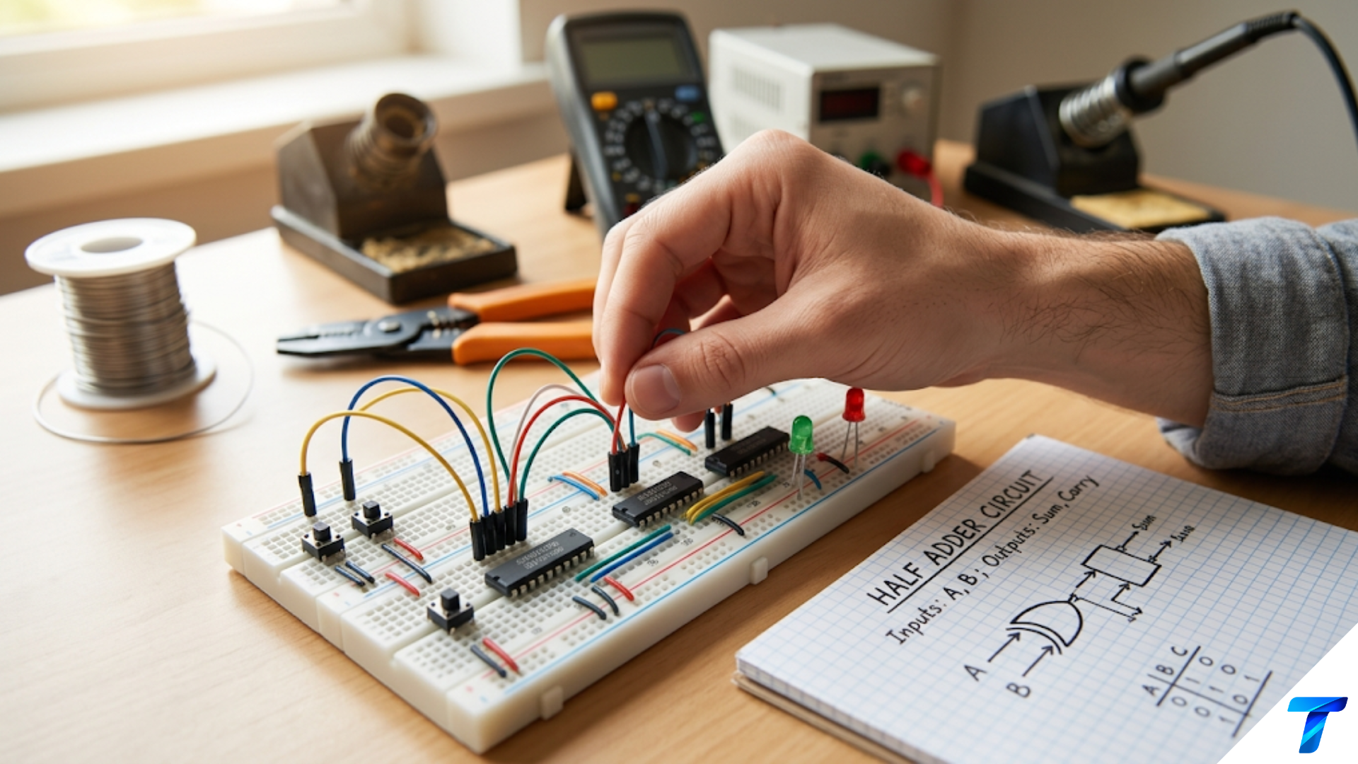
A half adder adds two single bits and produces a sum and carry:
Inputs: A, B
Outputs: SUM = A ⊕ B, CARRY = A · BGate implementation:
- Gate 1 (XOR): A, B → SUM
- Gate 2 (AND): A, B → CARRY
Two gates, two outputs. The simplest arithmetic circuit in existence.
ICs: One gate from a 74HC86 (XOR) + one gate from a 74HC08 (AND).
Limitation: The half adder cannot handle a carry-in from a previous bit position. For multi-bit addition, a full adder (which adds three inputs: A, B, and carry-in) is needed. The full adder uses two half adders plus an OR gate and is covered in Article 83.
From Half Adder to Arithmetic Logic Units
The half adder’s XOR+AND structure is the atomic unit of all digital arithmetic. A 4-bit ripple-carry adder uses four full adders chained together — carry-out of each bit feeds carry-in of the next. An 8-bit adder uses eight full adders. Modern CPUs use optimized adder structures (carry-lookahead, carry-select) that are fundamentally composed of XOR and AND gates at the bit level, just with smarter carry propagation.
Every addition, subtraction (using two’s complement representation), multiplication (repeated addition), and division operation in every processor ultimately reduces to XOR and AND operations on individual bits.
Application 2: Parity Generation and Checking
What Is Parity?
Parity is a simple error detection scheme: add one extra bit (the parity bit) to a data word such that the total number of 1-bits in the word (including the parity bit) is always even (even parity) or always odd (odd parity). At the receiver, recount the 1-bits. If the parity is wrong, at least one bit was corrupted in transmission.
Even parity: Total count of 1-bits = even. Parity bit set to make total even. Odd parity: Total count of 1-bits = odd. Parity bit set to make total odd.
Example — even parity for 8-bit data 0b10110100: Count of 1s: bits 1, 2, 4, 7 (0-indexed from right) = 4 ones (already even). Even parity bit P = 0 (no change needed; total remains 4 = even).
Data with parity: 0b10110100 P=0.
Example — even parity for 0b10110110: Count of 1s: positions 1, 2, 4, 5, 7 = 5 ones (odd). Even parity bit P = 1 (makes total 6 = even).
XOR as a Parity Calculator
The XOR of all data bits equals 1 when the number of 1-bits is odd, and 0 when even. This is exactly the even-parity bit value:
P_even = D7 ⊕ D6 ⊕ D5 ⊕ D4 ⊕ D3 ⊕ D2 ⊕ D1 ⊕ D0
For odd parity: invert the even parity bit:
P_odd = ̄(D7 ⊕ D6 ⊕ D5 ⊕ D4 ⊕ D3 ⊕ D2 ⊕ D1 ⊕ D0)Hardware 8-Bit Parity Generator
Implementation using three 74HC86 ICs (12 XOR gates for 8 inputs):
Tree structure (minimize gate levels for speed):
Level 1 (4 XOR gates, simultaneous):
- X1 = D0 ⊕ D1
- X2 = D2 ⊕ D3
- X3 = D4 ⊕ D5
- X4 = D6 ⊕ D7
Level 2 (2 XOR gates):
- X5 = X1 ⊕ X2
- X6 = X3 ⊕ X4
Level 3 (1 XOR gate):
- P_even = X5 ⊕ X6
Total: 7 XOR gates, 3 gate levels, propagation delay = 3 × 8ns = 24ns.
ICs: Two 74HC86 packages (8 gates total — use 7, one spare).
For odd parity: Add one more gate from 74HC04 to invert P_even → P_odd.
Parity Checking at the Receiver
The receiver recomputes the parity over all received bits including the transmitted parity bit:
CHECK = D7_recv ⊕ D6_recv ⊕ ... ⊕ D0_recv ⊕ P_recvIf no errors: CHECK = 0 (even parity — all 1s including parity bit sum to even). If one-bit error: CHECK = 1 (one extra 1-bit flips the parity).
Error syndrome: CHECK = 1 indicates an odd number of bit errors (1, 3, 5…). CHECK = 0 indicates no error or an even number of errors (2, 4, 6… — undetected). Parity can detect any single-bit error but cannot detect 2-bit errors.
Limitation: Parity indicates THAT an error occurred, not WHERE. It cannot correct the error — for error correction, more sophisticated codes (Hamming, Reed-Solomon) are needed, though they still use XOR as a fundamental operation.
Parity in Real Systems
Parity checking is used in:
- UART serial communication: Even or odd parity bit appended to each 8-bit character, checked at the receiver. Still used in industrial serial communications (RS-232, RS-485 with parity enabled).
- DRAM memory: Many server memory modules use ECC (Error Correcting Code), an extension of parity that both detects and corrects single-bit errors.
- Storage systems: RAID 5 and RAID 6 use XOR-based parity across multiple disks, allowing recovery if one or two disks fail.
- CAN bus: The 15-bit CRC (Cyclic Redundancy Check) in automotive CAN frames uses XOR-based polynomial division.
Application 3: Cyclic Redundancy Check (CRC) — Powerful Error Detection
Beyond Simple Parity
Parity detects only odd numbers of bit errors. For more robust error detection in data communications and storage, CRC (Cyclic Redundancy Check) uses a polynomial division algorithm that can detect all single-bit errors, all double-bit errors, all odd numbers of errors, and all burst errors up to a certain length.
XOR as Modulo-2 Division
CRC computes the remainder when the data polynomial is divided by a generator polynomial, where all arithmetic is modulo-2 (XOR instead of subtraction). The remainder is the CRC value appended to the transmitted data.
Modulo-2 division uses XOR: At each step of the polynomial long division, instead of subtracting (which would require borrowing), the divisor is XOR’d with the current portion of the dividend. This is why CRC circuits are built from XOR gates and shift registers.
Hardware CRC-8 Generator
For CRC-8 with polynomial x^8 + x^2 + x + 1 (used in some 1-Wire and SMBus applications):
The hardware implementation uses an 8-bit Linear Feedback Shift Register (LFSR) with XOR feedback at specific tap positions (taps at bits 2, 1, and 0 for this polynomial):
Data in → ⊕ → [B7][B6][B5][B4][B3][B2][B1][B0]
                                    ↑   ↑   ↑
                                    |   |   |
XOR feedback tapsAfter clocking all data bits through, the register contains the 8-bit CRC remainder. At the receiver, CRC is recomputed and compared to the received CRC field — a mismatch indicates corruption.
The hardware uses eight flip-flops and XOR gates at the feedback taps. The exact number of XOR gates equals the number of 1-bits in the generator polynomial minus 1 (the leading term).
CRC in Practice
| CRC Standard | Width | Generator Polynomial | Used In |
|---|---|---|---|
| CRC-8 | 8 bits | x^8+x^2+x+1 | 1-Wire, SMBus |
| CRC-16 | 16 bits | x^16+x^15+x^2+1 | USB, Modbus, HDLC |
| CRC-32 | 32 bits | x^32+x^26+x^23+… | Ethernet, ZIP, PNG |
| CRC-32C | 32 bits | Castagnoli polynomial | iSCSI, SCTP, SSE4.2 |
CRC-32 (IEEE 802.3) detects all single and double-bit errors, all errors in an odd number of bits, all burst errors of length ≤ 32 bits, and most longer burst errors. Modern processors include hardware CRC instructions (SSE4.2’s CRC32 instruction on x86) that compute CRC-32C in a single clock cycle using XOR logic at the hardware level.
Application 4: Digital Comparators
Bit-by-Bit Equality Detection
To compare two N-bit numbers for equality, compare each bit position independently using XNOR (equality gate), then AND all results:
EQUAL = (A7 ☉ B7) · (A6 ☉ B6) · ... · (A0 ☉ B0)All bit positions must match simultaneously (XNOR → HIGH when equal, AND requires all HIGH).
4-Bit Equality Comparator
Gate implementation:
- Four XNOR gates: one per bit position, output HIGH when bits match
- One 4-input AND gate: output HIGH only when ALL four bit positions match
EQ0 = A0 ☉ B0    (XNOR)
EQ1 = A1 ☉ B1
EQ2 = A2 ☉ B2
EQ3 = A3 ☉ B3
EQUAL = EQ0 · EQ1 · EQ2 · EQ3Using XOR instead of XNOR:
XOR outputs HIGH when bits differ. Use NOR instead of AND on XOR outputs:
NEQ0 = A0 ⊕ B0    (XOR — HIGH when different)
NEQ1 = A1 ⊕ B1
NEQ2 = A2 ⊕ B2
NEQ3 = A3 ⊕ B3
EQUAL = ̄(NEQ0 + NEQ1 + NEQ2 + NEQ3) = NOR(NEQ0, NEQ1, NEQ2, NEQ3)“Equal when no bit differs” — OR all XOR outputs (any difference → HIGH), then invert.
ICs: 74HC86 (quad XOR, uses all 4 gates) + 74HC4002 (dual 4-input NOR, uses 1 gate). Total: 2 ICs.
Magnitude Comparison (A > B, A < B)
Full magnitude comparison (determining A > B, A = B, A < B) is more complex — requires checking from the most significant bit downward. The 74HC85 is a dedicated 4-bit magnitude comparator IC with three outputs (A>B, A=B, A<B) and cascading inputs for extending to wider numbers.
The 74HC85 uses XOR gates internally to detect bit differences at each position, then priority logic to determine which number is larger based on the most significant differing bit.
Application 5: XOR in Encryption and Cryptography
The Perfect Cipher: One-Time Pad
XOR is the foundation of the only provably perfect encryption scheme: the one-time pad. The principle:
Encryption: CIPHERTEXT = PLAINTEXT ⊕ KEY Decryption: PLAINTEXT = CIPHERTEXT ⊕ KEY
Because (A ⊕ B) ⊕ B = A (XOR’s own-inverse property), XOR’ing the ciphertext with the same key exactly recovers the plaintext. This works at the bit level: each plaintext bit is XOR’d with the corresponding key bit.
Why it’s perfectly secure: If the key is:
- Truly random
- At least as long as the plaintext
- Never reused
Then the ciphertext contains zero information about the plaintext — every possible plaintext of that length is equally probable as a source. This is mathematically proven security, unlike the computational security of modern ciphers.
Why it’s not used everywhere: The key must be as long as the message (a 1GB message needs a 1GB key), must be truly random (not pseudo-random), and must be shared securely before communication. These practical constraints limit one-time pad use to high-security, low-bandwidth applications (diplomatic communications, nuclear command systems).
XOR in Stream Ciphers
Modern stream ciphers (ChaCha20, RC4, Salsa20) generate a pseudo-random keystream and XOR it with the plaintext:
CIPHERTEXT[i] = PLAINTEXT[i] ⊕ KEYSTREAM[i]The keystream is generated from a shorter key (128 or 256 bits) using complex algorithms. The security depends on the keystream’s unpredictability, not on XOR itself — XOR is merely the final mixing step because its perfect statistical properties ensure the ciphertext is as random-looking as the keystream.
XOR masking in AES: The AES (Advanced Encryption Standard) block cipher uses XOR in its AddRoundKey step — XOR’ing each 16-byte data block with the round key. AES performs 10–14 rounds of operations, each including XOR, and the security comes from the combination, not XOR alone.
Hardware XOR for Fast Encryption
In hardware implementations, XOR gates are extremely fast (single gate delay) and area-efficient. A 128-bit XOR operation requires 128 XOR gates operating in parallel — one gate level, one propagation delay, maximum throughput. This is why XOR-based operations appear throughout hardware cryptographic accelerators.
Application 6: Gray Code and Binary Conversion
What Is Gray Code?
Gray code (also called reflected binary code) is a numbering system where consecutive integers differ in exactly one bit. Standard binary does not have this property — the transition from 3 (011) to 4 (100) changes three bits simultaneously.
4-bit Gray code vs. binary:
| Decimal | Binary | Gray Code |
|---|---|---|
| 0 | 0000 | 0000 |
| 1 | 0001 | 0001 |
| 2 | 0010 | 0011 |
| 3 | 0011 | 0010 |
| 4 | 0100 | 0110 |
| 5 | 0101 | 0111 |
| 6 | 0110 | 0101 |
| 7 | 0111 | 0100 |
| 8 | 1000 | 1100 |
In Gray code, adjacent values differ in only one bit — a property called unit distance. The transition 3→4 in Gray code (0010 → 0110) changes only bit 1. Compare to binary (0011 → 0100) which changes bits 0, 1, and 2.
Why Gray Code Matters: Rotary Encoders
Rotary encoders output a binary code representing shaft angle. If the encoder uses standard binary, then at the transition between counts (e.g., 3→4), multiple bits change simultaneously. Due to mechanical tolerances, the bits never change at exactly the same instant — for a moment, the encoder might read 3, then 5, then 4 (a momentary glitch). In precision instruments or safety-critical systems, this is unacceptable.
Gray code encoders never have this problem — only one bit changes at each step. Even if the transition takes a finite time, the output is always a valid code (either the value before or after the transition, never a spurious intermediate value).
Gray code is also used in Karnaugh maps (the column/row headers follow Gray code order — adjacent cells differ by one bit, which is exactly why K-map adjacency works).
Binary to Gray Code Conversion Using XOR
Converting binary (B3 B2 B1 B0) to Gray code (G3 G2 G1 G0):
G3 = B3
G2 = B3 ⊕ B2
G1 = B2 ⊕ B1
G0 = B1 ⊕ B0Rule: Each Gray code bit = corresponding binary bit XOR’d with the next-higher binary bit. The MSB is unchanged.
Gate implementation: Three XOR gates (one per bit except MSB) — extremely simple.
Verification: Binary 0110 (= decimal 6):
- G3 = B3 = 0
- G2 = B3 ⊕ B2 = 0 ⊕ 1 = 1
- G1 = B2 ⊕ B1 = 1 ⊕ 1 = 0
- G0 = B1 ⊕ B0 = 1 ⊕ 0 = 1
- Gray = 0101 ✓ (matches table above)
Gray Code to Binary Conversion
Converting Gray (G3 G2 G1 G0) back to binary:
B3 = G3
B2 = B3 ⊕ G2 = G3 ⊕ G2
B1 = B2 ⊕ G1 = G3 ⊕ G2 ⊕ G1
B0 = B1 ⊕ G0 = G3 ⊕ G2 ⊕ G1 ⊕ G0Rule: Each binary bit = XOR of all Gray code bits from MSB down to the current bit. This is a cascaded XOR — each bit depends on the previous result, making it inherently sequential.
Gate implementation:
- B3 = G3 (no gate)
- B2 = XOR(G3, G2) — 1 XOR gate
- B1 = XOR(B2, G1) — 1 XOR gate (uses B2, not G2)
- B0 = XOR(B1, G0) — 1 XOR gate
Three XOR gates in a chain — propagation delay is 3 × 8ns = 24ns for 74HC86.
Verification: Gray 0101 (= decimal 6):
- B3 = G3 = 0
- B2 = 0 ⊕ 1 = 1
- B1 = 1 ⊕ 0 = 1
- B0 = 1 ⊕ 1 = 0
- Binary = 0110 = decimal 6 ✓
Application 7: Linear Feedback Shift Register (LFSR)
What Is an LFSR?
A Linear Feedback Shift Register is a shift register (chain of flip-flops) where the input to the first stage is computed by XOR’ing certain output stages (the feedback taps). LFSRs generate pseudo-random binary sequences with extremely long periods using very simple hardware.
Structure and Operation
An N-bit LFSR consists of:
- N flip-flops connected in series (a shift register)
- XOR gates combining selected flip-flop outputs (the taps)
- The XOR output feeding back to the first flip-flop input
On each clock cycle:
- The XOR feedback is computed from the selected tap outputs
- All flip-flops shift right (or left) by one position
- The feedback value enters the first flip-flop
If the tap positions are chosen correctly (corresponding to a primitive polynomial), the LFSR cycles through all 2^N − 1 non-zero states before repeating — a maximal-length sequence (m-sequence). The sequence appears random but is completely deterministic and repeatable.
Maximal-Length LFSR Tap Positions
| LFSR Width | Taps (feedback bits) | Period (2^N−1) |
|---|---|---|
| 4-bit | [4,3] | 15 |
| 8-bit | [8,6,5,4] | 255 |
| 16-bit | [16,15,13,4] | 65,535 |
| 32-bit | [32,22,2,1] | 4,294,967,295 |
4-Bit LFSR Design Example
4-bit LFSR with taps at positions 4 and 3:
Flip-flops: Q4, Q3, Q2, Q1
Feedback: D4 = Q4 ⊕ Q3
Shift: D3 = Q4, D2 = Q3, D1 = Q2Starting from 0001 (initial state), the sequence cycles through all 15 non-zero states: 0001, 1000, 1100, 0110, 0011, 1001, 1100…
Let me trace carefully:
- State 1: Q4Q3Q2Q1 = 0001, feedback = Q4⊕Q3 = 0⊕0 = 0
- Shift: Q4←Q3=0, Q3←Q2=0, Q2←Q1=1, Q1←feedback=0 → 0010
Actually let me define the shift direction properly:
- D1 (new Q1) = feedback = Q4 ⊕ Q3
- D2 (new Q2) = Q1
- D3 (new Q3) = Q2
- D4 (new Q4) = Q3
State sequence starting from Q4Q3Q2Q1 = 0001:
- 0001: fb = 0⊕0 = 0 → next = 0000+0 = 0 shifts Q4Q3Q2 left…
Let me use a cleaner notation. Starting state 1 (binary 0001):
| Clock | Q4 | Q3 | Q2 | Q1 | Feedback (Q4⊕Q3) |
|---|---|---|---|---|---|
| 0 | 0 | 0 | 0 | 1 | 0 |
| 1 | 0 | 0 | 1 | 0 | 0 |
| 2 | 0 | 1 | 0 | 0 | 1 |
| 3 | 1 | 0 | 0 | 1 | 1 |
| 4 | 0 | 0 | 1 | 1 | 0 |
| 5 | 0 | 1 | 1 | 0 | 1 |
| 6 | 1 | 1 | 0 | 1 | 0 |
| 7 | 1 | 0 | 1 | 0 | 1 |
| 8 | 0 | 1 | 0 | 1 | 1 |
| 9 | 1 | 0 | 1 | 1 | 1 |
| 10 | 0 | 1 | 1 | 1 | 1 |
| 11 | 1 | 1 | 1 | 1 | 0 |
| 12 | 1 | 1 | 1 | 0 | 0 |
| 13 | 1 | 1 | 0 | 0 | 0 |
| 14 | 1 | 0 | 0 | 0 | 1 |
| 15 = 0 | 0 | 0 | 0 | 1 | (returns to start) |
All 15 non-zero 4-bit states appear exactly once before repeating — maximal-length sequence confirmed.
Gate implementation (4-bit LFSR):
- 4 D flip-flops (74HC74 contains 2; use two 74HC74s or one 74HC175 quad D flip-flop)
- 1 XOR gate (one gate from 74HC86)
- Clock input
Applications of LFSRs:
- Pseudo-random number generation in hardware (spread spectrum communications, white noise generation for testing)
- Built-in self-test (BIST) in digital ICs — LFSRs generate test patterns and compress response signatures
- Scrambling in serial data links (PCIe, USB 3, SATA) — XOR data with LFSR output to randomize bit patterns and prevent long runs of 0s or 1s that cause clock recovery problems
- Spread-spectrum clocking to reduce EMI peaks (vary clock frequency slightly using LFSR modulation)
- CRC generation (as described earlier — CRC circuits are equivalent to LFSRs with specific tap polynomials)
Application 8: Programmable Inverter (Controlled Complement)
XOR as a Conditional Inverter
From the identity A ⊕ 1 = Ā and A ⊕ 0 = A: XOR with a control bit either passes the data unchanged (control=0) or inverts it (control=1).
OUTPUT = DATA ⊕ CONTROLWhen CONTROL = 0: OUTPUT = DATA (pass through) When CONTROL = 1: OUTPUT = ̄DATA (invert)
This is a single-gate programmable inverter — a fundamental building block in arithmetic circuits and data path design.
Practical Applications
Two’s complement negation: To negate a number in two’s complement, invert all bits (XOR each with 1) then add 1. The “invert all bits” step uses XOR gates with a NEGATE control line:
B_inverted[i] = B[i] ⊕ NEGATEFor all 8 bits of an 8-byte number, 8 XOR gates with a shared NEGATE control implement the inversion step. Then adding 1 (handled by carry propagation with carry-in = NEGATE) completes the negation.
Adder/Subtractor circuit: An 8-bit adder with SUB control line:
- Each B input XOR’d with SUB: when SUB=0, B passes unchanged → addition
- When SUB=1, B is inverted → combined with carry-in of 1 → subtraction (two’s complement)
The 8 XOR gates at the B inputs form a programmable inverter bank, turning any adder into an adder/subtractor with a single control line. This exact circuit is inside every ALU (Arithmetic Logic Unit) in every processor.
Bidirectional data bus: XOR gates can implement bidirectional data paths where the direction of data flow (read vs. write) is controlled by a single direction bit.
Complete Design Example: 4-Bit Parity Checker/Generator System
Application: A complete system that both generates parity on the transmitter side and checks parity on the receiver side, using the same circuit. Input: 4 data bits (D3, D2, D1, D0) and a MODE signal. MODE=0: generate even parity bit P. MODE=1: check received parity (including received parity bit P_recv) and output ERROR signal.
Analysis:
Generator mode (MODE=0): P = D3 ⊕ D2 ⊕ D1 ⊕ D0
Checker mode (MODE=1): ERROR = D3 ⊕ D2 ⊕ D1 ⊕ D0 ⊕ P_recv (ERROR = 1 if total count of 1s is odd → parity error)
Both operations use the same XOR tree! The only difference is the interpretation of the output and whether P is an input or output.
Unified circuit:
X1 = D0 ⊕ D1          (XOR gate 1, from 74HC86 #1)
X2 = D2 ⊕ D3          (XOR gate 2)
X3 = X1 ⊕ X2          (XOR gate 3 — XOR of all four data bits)
X4 = X3 ⊕ P_recv (XOR gate 4 — include received parity)In generator mode: ignore P_recv (tie to 0 or leave X4 unused), output X3 as parity P. In checker mode: input P_recv, output X4 as ERROR flag.
Complete circuit for one system (uses both modes):
- XOR gates 1–3: tree computing D3⊕D2⊕D1⊕D0
- XOR gate 4: adds P_recv to get ERROR check result
- Multiplexer (or separate outputs): select between generator output (X3) and checker output (X4)
ICs: Two 74HC86 (quad XOR) packages — uses 4 of 8 available XOR gates. One 74HC157 (quad 2:1 multiplexer) for MODE selection, or simply bring both outputs to separate pins and let the system use whichever is relevant.
Gate total: 4 XOR gates + 1 MUX (if needed) = 2–3 ICs.
Verification (generator mode): D = 1011 (D3=1, D2=0, D1=1, D0=1):
- X1 = 1⊕1 = 0
- X2 = 0⊕1 = 1
- X3 = 0⊕1 = 1 → P_even = 1
Check: 1,0,1,1 has three 1s (odd). Even parity bit = 1 makes total four 1s (even). ✓
Verification (checker mode): Received: D = 1011, P_recv = 1 (correct transmission):
- X3 = 1 (as computed above)
- X4 = 1 ⊕ 1 = 0 → ERROR = 0 ✓ (no error)
Received with bit error: D = 1001 (bit 1 flipped), P_recv = 1:
- X1 = 1⊕0 = 1
- X2 = 0⊕1 = 1
- X3 = 1⊕1 = 0
- X4 = 0⊕1 = 1 → ERROR = 1 ✓ (error detected!)
XOR in Modern Digital Systems: A Summary of Roles
| Application | XOR Role | Why XOR Is Ideal |
|---|---|---|
| Binary addition (half adder) | Computes sum bit | XOR = addition mod 2 |
| Full adder | Sum computation | Cascaded XOR with carry |
| Parity generation | XOR of all data bits | Multi-input XOR = odd parity |
| CRC generation | Polynomial division feedback | Modulo-2 arithmetic = XOR |
| Digital comparator | Bit equality check | XNOR detects match |
| Gray code conversion | Adjacent code generation | Unit-distance property |
| LFSR (pseudo-random) | Feedback computation | XOR maintains sequence length |
| Encryption (stream cipher) | Data XOR keystream | XOR is its own inverse |
| Adder/subtractor | Programmable inversion | A⊕1=Ā, A⊕0=A |
| Error correction (Hamming) | Syndrome computation | XOR linearity enables ECC |
| RAID parity | Disk redundancy | XOR parity across disks |
Common Mistakes with XOR Gates
Mistake 1: Confusing XOR with OR for “at least one HIGH” detection OR outputs HIGH when any input is HIGH, including when both are HIGH. XOR excludes the “both HIGH” case. For “either A or B (but not both)” use XOR. For “either A or B (including both)” use OR.
Mistake 2: Using XNOR incorrectly for equality XNOR output is HIGH when inputs MATCH. Using XOR and expecting HIGH for equality will give the opposite result. When building comparators, use XNOR gates (or XOR followed by NOT) for each bit position.
Mistake 3: Cascading XOR incorrectly for parity The associative property of XOR allows any grouping, but the tree structure (multiple XOR stages) introduces gate delays. For timing-critical designs, minimize the number of gate levels — use a balanced binary tree structure rather than a linear chain.
Mistake 4: Wrong LFSR initialization An LFSR initialized to all-zeros (0000…0) will stay all-zeros forever (XOR of zeros is zero). Always initialize to any non-zero value. Most hardware LFSR implementations use a preset circuit that forces the all-ones state on power-up.
Mistake 5: Reusing an XOR key XOR encryption (one-time pad, stream cipher) is secure only when the key is never reused. If two messages are encrypted with the same keystream (KEY_A ⊕ MSG1 and KEY_A ⊕ MSG2), an attacker can XOR the two ciphertexts to get MSG1 ⊕ MSG2 — the key cancels out. Many real-world encryption failures have resulted from reusing keys or IVs in XOR-based ciphers.
Summary
XOR’s defining property — output HIGH when inputs differ — makes it uniquely useful across an extraordinary breadth of digital applications. Its mathematical properties (commutative, associative, self-inverse, own-inverse, identity with 0, inversion with 1) give it capabilities that no other single gate type possesses.
In arithmetic, XOR computes the sum bit of binary addition without carry — the atomic operation in every adder and ALU. In error detection, cascaded XOR computes parity over any number of bits in a tree structure with logarithmic gate depth. In Gray code conversion, three XOR gates convert binary to unit-distance encoding or back, enabling glitch-free rotary encoder readout. In LFSRs, a single XOR gate at the feedback creates pseudo-random sequences of period up to 2^N − 1.
As a programmable inverter (A ⊕ CONTROL), XOR enables single-wire control of signal polarity — the foundation of adder/subtractor circuits, encryption mixing, and data scrambling. As an equality detector (in XNOR form), it enables magnitude comparators and address matching. In CRC computation, XOR implements modulo-2 polynomial division that detects virtually all real-world data errors.
The 74HC86 quad XOR IC is the practical implementation — four independent 2-input XOR gates in a standard 14-pin package, directly interchangeable in footprint with other 7400-series ICs, propagation delay 8ns at 5V.