An H-bridge circuit uses four switching devices — typically MOSFETs — arranged in a configuration that allows current to flow through a motor in either direction, enabling forward rotation, reverse rotation, active braking, and coasting. Named for its resemblance to the letter H when drawn schematically, the H-bridge is the fundamental building block of all bidirectional DC motor controllers, from tiny hobby robot drivers to industrial servo amplifiers.
Introduction: The Circuit That Gives Motors Direction
A simple transistor switch can turn a motor on and off. It can even control speed with PWM. But it cannot reverse the motor — current always flows in the same direction through the motor winding. For a robot that needs to drive forward and backward, a conveyor that must run in both directions, a valve actuator that must open and close, or any application requiring bidirectional motion, a single transistor switch is fundamentally insufficient.
The H-bridge solves this problem with elegant simplicity. By placing four switches around a motor in a specific arrangement, current can be routed through the motor in either direction. Close switches 1 and 4: current flows left to right through the motor (forward). Open those, then close switches 2 and 3: current flows right to left (reverse). The motor experiences the same supply voltage but with reversed polarity — it runs in the opposite direction.
This topological insight — four switches arranged to reverse a load’s polarity — is one of the most useful circuit concepts in all of power electronics. Beyond DC motor control, the same H-bridge topology (sometimes called a full bridge) forms the basis of single-phase inverters (converting DC to AC), class D audio amplifiers (switching audio power amplifiers), and DC-DC converters. Mastering the H-bridge means mastering a fundamental power electronics building block.
This article provides a complete treatment of H-bridge circuits for DC motor control: the topology and operating modes, the critical safety concern of shoot-through and how to prevent it, PWM speed control through the H-bridge, freewheeling and braking modes, gate drive requirements for the four-switch bridge, selecting between discrete MOSFET bridges and integrated H-bridge ICs, thermal management, and four complete design examples spanning hobby robotics to professional motor drives.
The H-Bridge Topology
Circuit Structure
Draw four switches — call them Q1, Q2, Q3, Q4 — arranged as follows:
V_supply
    |
   Q1 (high-side left)      Q3 (high-side right)
    |                               |
    +------- Motor --------+
    |                               |
   Q2 (low-side left)       Q4 (low-side right)
    |                               |
GND GNDMore precisely:
- Q1: High-side left — connects V_supply to the left motor terminal
- Q2: Low-side left — connects the left motor terminal to GND
- Q3: High-side right — connects V_supply to the right motor terminal
- Q4: Low-side right — connects the right motor terminal to GND
The motor sits horizontally between the two “legs” of the bridge. The vertical power rails (V_supply at top, GND at bottom) and the horizontal motor connection form the letter H — hence the name.
Operating Modes
The four switches can be set to five useful states:
Mode 1: Forward (Q1 + Q4 on, Q2 + Q3 off)
- Left motor terminal: connected to V_supply through Q1
- Right motor terminal: connected to GND through Q4
- Current flows: V_supply → Q1 → Motor (left to right) → Q4 → GND
- Motor rotates forward
Mode 2: Reverse (Q2 + Q3 on, Q1 + Q4 off)
- Left motor terminal: connected to GND through Q2
- Right motor terminal: connected to V_supply through Q3
- Current flows: V_supply → Q3 → Motor (right to left) → Q2 → GND
- Motor rotates backward
Mode 3: Coast / Free-wheel (all switches off)
- Both motor terminals floating
- Motor current decays slowly through body diodes if still spinning
- Motor coasts to a stop — no active deceleration
- Lowest power dissipation during “stop”
Mode 4: Active Brake — Low-Side (Q2 + Q4 on, Q1 + Q3 off)
- Both motor terminals connected to GND
- Motor acts as a generator: back-EMF drives current through the short circuit (Q2 + Q4)
- Current circulates: Motor → Q4 → GND → Q2 → Motor
- Rapid deceleration — motor is short-circuited and slows quickly
- Energy dissipated in motor winding resistance and MOSFET on-resistance
Mode 5: Active Brake — High-Side (Q1 + Q3 on, Q2 + Q4 off)
- Both motor terminals connected to V_supply
- Same short-circuit braking effect but current path through high-side switches
- Less commonly used than low-side braking
The distinction between coast and active brake is important for many applications. A robot arm that must hold position needs active braking to resist being back-driven. A conveyor that must stop quickly needs active braking. A battery-powered device that must minimize power consumption might prefer coasting.
The Deadly Forbidden State: Shoot-Through
There is a sixth state that must NEVER occur:
Forbidden: Q1 + Q2 on simultaneously (left leg shoot-through)
If both Q1 and Q2 conduct simultaneously, V_supply is connected directly to GND through the left leg:
Current path: V_supply → Q1 → Q2 → GNDThe only thing limiting this current is the on-resistance of Q1 and Q2 plus trace resistance — typically milliohms total. With a 12V supply and 10mΩ total resistance:
I_shoot = 12V / 0.010Ω = 1,200ATwelve hundred amps flows for as long as shoot-through lasts — typically until something explodes. MOSFETs are destroyed in microseconds. PCB traces vaporize. Capacitors rupture. In a best-case scenario, a fuse opens quickly enough to save the rest of the circuit.
The same catastrophic result occurs if Q3 + Q4 conduct simultaneously (right leg shoot-through).
Preventing shoot-through is the primary safety concern in every H-bridge design. Every legitimate H-bridge design — from a $0.50 hobby IC to a $500 industrial motor driver — includes shoot-through protection as a fundamental requirement.
Shoot-Through Prevention: Deadtime and Interlocking
Hardware Deadtime
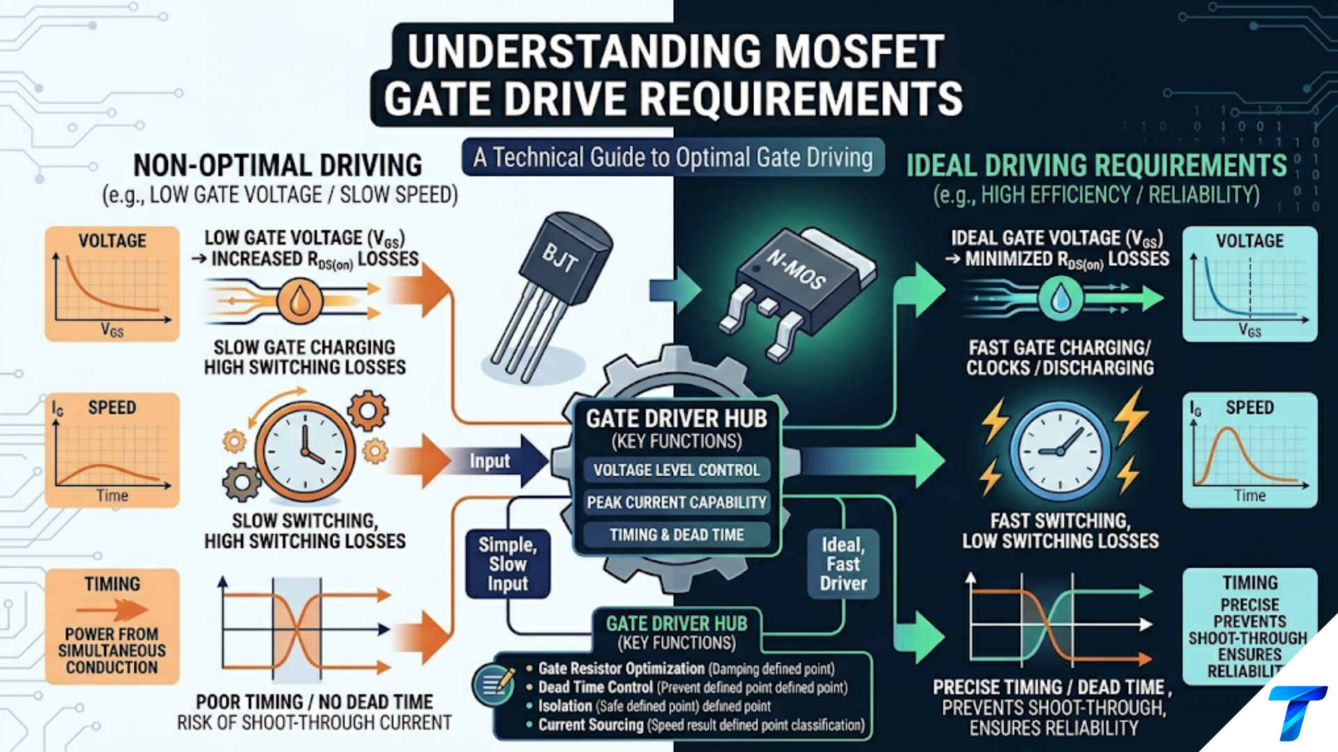
As covered in the previous article on MOSFET gate drive, deadtime is a brief period between turning off one switch and turning on the complementary switch. In an H-bridge leg:
- Q1 turns off (gate driven to 0V)
- Wait: t_deadtime (both Q1 and Q2 are off — deadtime period)
- Q2 turns on (gate driven to V_GS)
The deadtime must be at least as long as the slowest switch’s turn-off time:
t_deadtime ≥ max(t_off_Q1, t_off_Q2) + safety_marginFor MOSFETs with 100ns turn-off times: t_deadtime ≥ 200–300ns typically.
Many H-bridge driver ICs implement deadtime internally, automatically inserting the required delay between complementary switch transitions. The IR2104 inserts 520ns of fixed deadtime. The DRV8833 inserts adjustable deadtime. When using discrete gate drivers, deadtime must be added by the PWM controller or implemented in hardware.
Logic Interlocking
Beyond deadtime (which prevents simultaneous switching during transitions), hardware interlocking prevents shoot-through from incorrect control signals. A simple AND/OR gate logic circuit can ensure that if both high-side and low-side inputs are asserted simultaneously, neither switch turns on.
Half-bridge interlock using logic:
Q1_gate_enable = IN_high AND NOT(IN_low)
Q2_gate_enable = IN_low AND NOT(IN_high)If both IN_high and IN_low are asserted: both Q1_gate_enable and Q2_gate_enable go LOW — neither switch turns on. The circuit fails safe to the coast (all off) state.
Most integrated H-bridge driver ICs implement this interlocking in silicon, making the bridge inherently safe against incorrect control inputs.
Undervoltage Lockout (UVLO)
During power-up and power-down, supply voltage ramps up or down slowly. During this time, gate drive voltage may be insufficient to fully enhance the MOSFETs, leaving them in the linear region with high R_DS(on) and high dissipation. Worse, bootstrap capacitors may not be properly charged, causing unpredictable high-side switch behavior.
Undervoltage lockout (UVLO) disables all gate drive outputs when the gate driver’s supply voltage falls below a threshold (typically 8–10V for 10V-rated gate drivers). The switches remain off until the supply is firmly established. UVLO is standard in all professional gate driver ICs and is an essential safety feature.
PWM Speed Control Through an H-Bridge
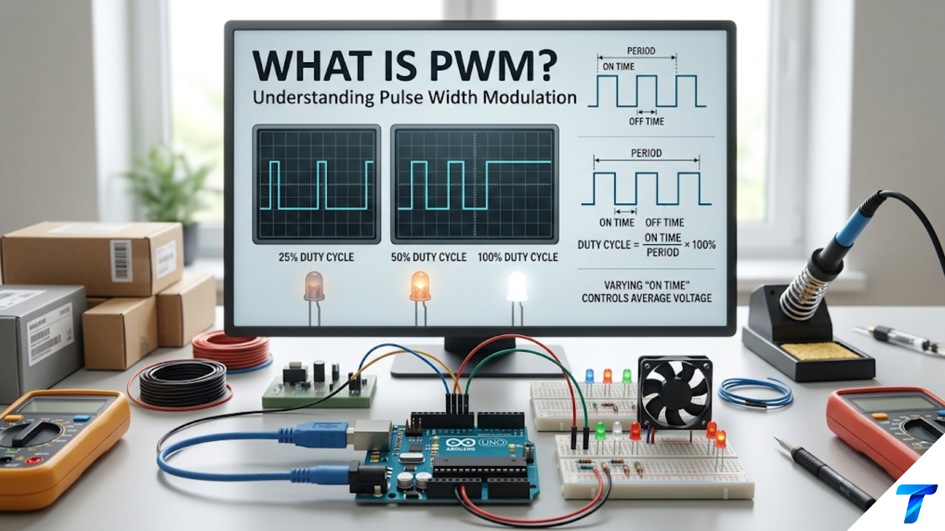
An H-bridge is most useful when combined with PWM (Pulse-Width Modulation) to control motor speed continuously from zero to full speed in either direction.
PWM Modulation Schemes
Several PWM strategies can be applied to an H-bridge. Each has different characteristics in terms of switching losses, motor current ripple, acoustic noise, and control complexity.
Scheme 1: Sign-Magnitude (Unipolar) PWM
One diagonal pair (Q1 + Q4 for forward, Q2 + Q3 for reverse) is fixed on to set direction, while the other diagonal is PWM-modulated for speed. This is the simplest scheme:
- Forward direction: Q1 always on, Q4 PWM’d
- When Q4 is on: full current flows through Q1 → Motor → Q4 (powered stroke)
- When Q4 is off: motor current freewheels through Q1 and Q3’s body diode (circulating in the top of the bridge)
Advantages: Simple control — one switch does the PWM switching, direction set separately. Disadvantages: High switching losses on the PWM switch; motor sees voltage swings from 0 to V_supply.
Scheme 2: Lock-Antiphase (Bipolar) PWM
Both diagonals are switched simultaneously: Q1+Q4 on for the positive half-cycle, Q2+Q3 on for the negative half-cycle. The duty cycle of each determines the net motor voltage:
V_motor_average = V_supply × (2D − 1)Where D is the duty cycle of the Q1+Q4 phase. At D = 0.5 (50%): V_motor_average = 0 (motor stopped). At D = 0.75: V_motor_average = +0.5 × V_supply (half forward speed). At D = 0.25: V_motor_average = −0.5 × V_supply (half reverse speed).
Advantages: Smooth zero-speed crossing (no dead zone), good low-speed torque, natural regenerative braking through the bridge. Disadvantages: Both legs switch every cycle — four switching events per PWM period instead of two. Higher total switching losses. Motor sees voltage swing from −V_supply to +V_supply on every cycle — higher current ripple and magnetic losses.
Scheme 3: Independent PWM with Freewheeling (Synchronous Rectification)
The most efficient scheme for modern motor drives. All four switches are controlled independently:
- During powered stroke: Q1 + Q4 on (or Q2 + Q3 for reverse)
- During freewheeling: Q2 + Q4 on (both low-side switches on — low-side circulating braking)
- Or for regenerative freewheeling: Q1 + Q3 on (both high-side switches on)
Using the low-side switches to provide the freewheeling path instead of body diodes reduces freewheeling losses from ~0.7V × I to R_DS(on) × I — significant at high currents where body diode drop is wasteful.
This synchronous rectification approach requires precisely coordinated gate timing and deadtime management but dramatically improves efficiency at high currents.
PWM Frequency Selection
The PWM frequency affects motor performance, switching losses, and acoustic noise:
Too low (< 1kHz): Motor current ripple is large — the motor current has time to rise substantially during each on-pulse, causing jerky motion at low speeds. PWM noise is audible (buzzing, whining). Some motors vibrate excessively at resonant frequencies in the audio range.
Optimal for motors (1kHz to 20kHz): Good current ripple (typically < 20% of rated current with adequate motor inductance). Below 20kHz, PWM noise may still be audible in some motors. Switching losses manageable.
Above 20kHz (ultrasonic): PWM noise is inaudible (above human hearing range). Motor runs silently. Higher switching losses — adequate for small motors and efficiency-sensitive designs, less appropriate for very high current applications.
Above 100kHz: Switching losses become dominant for most power MOSFETs. Requires careful gate drive design and low-Q_g MOSFETs. Used in very compact, high-performance designs.
PWM frequency and motor inductance: The motor winding inductance determines current ripple:
ΔI_ripple = (V_supply × D × (1−D)) / (L_motor × f_PWM)For V_supply = 12V, D = 0.5, L_motor = 1mH, f_PWM = 20kHz:
ΔI_ripple = (12 × 0.5 × 0.5) / (0.001 × 20,000) = 3V / 20 = 0.15A15% ripple on a 1A motor — acceptable. At f_PWM = 1kHz:
ΔI_ripple = 3V / 1 = 3A — extremely high ripple, unacceptableHigher inductance motors or higher switching frequencies reduce ripple.
Freewheeling and Regenerative Braking
What Happens When a Switch Opens Under Load
When the powered diagonal (Q1 + Q4) turns off during PWM operation, the motor’s inductive winding still has current flowing through it. This current must continue — inductors resist instantaneous current change. The current finds a path through the bridge’s body diodes (or synchronously through the low-side switches if synchronous rectification is used).
Freewheeling current path (Q1 + Q4 turning off, forward rotation):
The motor current was flowing: V_supply → Q1 → Motor → Q4 → GND (left to right through motor).
When Q1 and Q4 open:
- Motor winding acts as a current source (left terminal is now negative relative to right — back-EMF from inductance)
- Current flows: Motor (left terminal) → D_Q2 body diode of Q2 (anode at left terminal, cathode at V_supply rail) → back through motor
Wait — let me trace this correctly:
Motor current was flowing left to right (entering left terminal, exiting right terminal to Q4/GND). When Q4 turns off:
- Right terminal of motor tries to rise (inductor maintains current direction — current was flowing out of right terminal into GND through Q4, so right terminal tries to go negative when Q4 opens)
- D_Q4 body diode conducts: right terminal → D_Q4 body diode → GND (anode at right motor terminal, cathode… no, body diode of Q4 is from source (GND) to drain (motor right terminal))
Let me re-examine: For an N-channel MOSFET, the body diode has its anode at the source and cathode at the drain. For Q4 (low-side right): source = GND, drain = right motor terminal. Body diode anode = GND, cathode = right motor terminal. This diode conducts when drain (right motor terminal) goes BELOW source (GND) — i.e., when right terminal goes negative.
When Q4 opens and motor tries to maintain current flowing out of its right terminal (current was flowing from right terminal to GND through Q4): right terminal goes negative → Q4 body diode conducts from GND to right motor terminal ✓. Current continues flowing from right terminal through body diode to GND.
And for the left side: current was entering left terminal from Q1 (V_supply). Now Q1 opens. Left terminal tries to go positive (inductor maintains current flowing into left terminal). Q1 body diode: source = left motor terminal (in this high-side configuration source is at switching node = left motor terminal), drain = V_supply. Body diode anode = source = left motor terminal, cathode = drain = V_supply. This conducts when left motor terminal > V_supply. With the inductor pushing left terminal positive, it exceeds V_supply by one diode drop and Q1’s body diode conducts.
Complete freewheeling path: GND → Q4 body diode → Right motor terminal → through motor → Left motor terminal → Q1 body diode → V_supply rail → through supply capacitor → GND.
The motor current circulates through the supply rail — the motor is actually returning energy to the supply capacitor during freewheeling (regenerative). This is normal and beneficial — the supply capacitor stores the energy rather than dissipating it in resistors.
Regenerative Braking Through an H-Bridge
When a DC motor is driven by mechanical means (shaft spun externally), it generates a back-EMF voltage. If the H-bridge is configured to allow this generated current to flow back into the supply, the motor acts as a generator and braking is regenerative — energy is returned to the source rather than wasted as heat.
How to implement regenerative braking:
While the motor is spinning forward (left-to-right current), open Q4 (or Q1), allowing the motor’s back-EMF to push current back through the body diodes (or synchronous switches) into the supply capacitor. If the supply is a battery, the battery is recharged — genuine energy recovery.
The condition for regenerative braking: the motor’s back-EMF must exceed the supply voltage for current to flow back into the supply. If back-EMF < V_supply (motor spinning slowly), regeneration is not possible — the motor simply coasts.
In bipolar PWM (lock-antiphase): Regenerative braking occurs naturally whenever the duty cycle commands less voltage than the motor’s back-EMF. This is one of the key advantages of bipolar PWM — smooth, automatic regenerative braking without mode switching.
High-Side Gate Drive in H-Bridges
Both high-side switches (Q1 and Q3) require above-rail gate drive voltages — the same challenge described in the previous article. In an H-bridge, both high-side switches need bootstrap or charge pump supplies.
Two Bootstrap Circuits for a Full H-Bridge
A full H-bridge requires two independent bootstrap circuits — one for Q1 (high-side left) and one for Q3 (high-side right). Each bootstrap capacitor charges independently during its respective low-side switch’s on-time:
- C_boot_left charges when Q2 is on (left leg switching node = GND)
- C_boot_right charges when Q4 is on (right leg switching node = GND)
In normal PWM operation with sign-magnitude scheme, Q4 switches while Q1 is held on. During this operation:
- C_boot_right refreshes every time Q4 turns on
- C_boot_left: Q2 is off (Q1 is on), so C_boot_left never gets to recharge!
This is a fundamental constraint: the high-side switch’s bootstrap capacitor only recharges when the complementary low-side switch conducts. If Q1 stays on continuously (100% duty cycle on the left leg), C_boot_left discharges and eventually Q1 loses gate drive.
Solution for sign-magnitude PWM: Use Q4 for PWM switching (not Q1). Keep Q1 always on. Then C_boot_left can charge through an alternate path, or — more practically — accept that the left high-side bootstrap cannot sustain 100% duty cycle indefinitely. Most applications stay below 95% duty cycle.
Alternative solution: Use a P-channel MOSFET for the high-side switches. P-channel MOSFETs require only a negative V_GS (gate below source), which can be generated from the existing supply without bootstrap complexity. The trade-off: P-channel MOSFETs have higher R_DS(on) for the same die size and cost more.
Integrated Half-Bridge Driver with Bootstrap
The IR2104 (described in the previous article) drives one half-bridge (one high-side + one low-side MOSFET) with a single input and built-in 520ns deadtime. For a full H-bridge, two IR2104s are needed:
- IR2104 #1: Drives Q1 (high-side left) + Q2 (low-side left)
- IR2104 #2: Drives Q3 (high-side right) + Q4 (low-side right)
Control: The IN pin of IR2104 #1 sets the left leg state; IN of IR2104 #2 sets the right leg state. For forward drive: IN_1 = HIGH (Q1 on, Q2 off), IN_2 = LOW (Q3 off, Q4 on). For reverse: IN_1 = LOW, IN_2 = HIGH. For brake: both INs LOW or both HIGH.
Integrated H-Bridge Driver ICs
For most applications, integrated H-bridge ICs are preferred over discrete MOSFETs + gate driver ICs. They integrate protection, deadtime, logic interfacing, and sometimes the MOSFETs themselves into a single package, dramatically simplifying design.
Comparison of Popular H-Bridge ICs
| IC | Voltage | Current | R_DS(on) | Control Interface | Protection | Package |
|---|---|---|---|---|---|---|
| L293D | 4.5–36V | 0.6A | 70Ω (high!) | IN1/IN2/EN | Thermal | DIP-16 |
| L298N | 4.5–46V | 2A | 2Ω | IN1/IN2/EN | Thermal | Multiwatt |
| DRV8833 | 2.7–10.8V | 1.5A | 0.36Ω | IN1/IN2/IN3/IN4 | OCP, thermal | WSON-16 |
| DRV8871 | 6.5–45V | 3.6A | 0.565Ω | IN1/IN2 | OCP, thermal | HSOP-8 |
| TB6612FNG | 2.7–13.5V | 1.2A | 0.5Ω | IN1/IN2/PWM | OCP, thermal | SSOP-24 |
| VNH5019 | 5.5–24V | 12A | 0.034Ω | INA/INB/PWM | OCP, thermal, diag. | MULTIWATT |
| DRV8432 | 8–52V | 7A | 0.17Ω | PWM H/L | OCP, UVLO | HTSSOP |
The L293D: Why You Should Usually Avoid It
The L293D is the classic H-bridge IC taught in nearly every introductory robotics course. While it works, its 70Ω internal switch resistance makes it a poor choice for almost any real application:
At 0.5A (near its rated current): V_drop = 0.5A × 70Ω = 35V dropped across the switch! For a 6V supply: the motor only sees 6V − 35V = −29V… clearly the L293D cannot handle anywhere near 1A into a real motor at reasonable supply voltages.
In practice, L293D is limited to about 100–200mA actual motor current before the internal drops make it inefficient. For any serious motor control application, use the DRV8833, TB6612FNG, or VNH5019 depending on current requirements.
DRV8833: The Modern Hobbyist Standard
The DRV8833 (Texas Instruments) contains two full H-bridges (can drive two motors or one stepper motor) with modern N-channel MOSFET technology:
- Supply: 2.7V to 10.8V — works with 3.3V, 5V, and up to 10V systems
- Current: 1.5A per bridge (2A peak) — adequate for most small motors
- R_DS(on): 360mΩ total (high + low side combined) — far superior to L293D
- Control: Each bridge controlled by two logic inputs (xIN1, xIN2) per the truth table below
- Protection: Overcurrent, thermal shutdown, undervoltage lockout
DRV8833 Truth Table:
| xIN1 | xIN2 | Motor State |
|---|---|---|
| 0 | 0 | Coast (all switches off) |
| 0 | 1 | Forward |
| 1 | 0 | Reverse |
| 1 | 1 | Brake (low-side short) |
Standby mode: Pull nSLEEP LOW to put the device in sleep mode (< 1µA). Pull HIGH to enable. Essential for battery-powered applications.
PWM control: Apply PWM to xIN1 while holding xIN2 HIGH (or vice versa). The DRV8833 automatically handles the complementary switching with internal deadtime.
TB6612FNG: Dual Motor Driver with PWM Pin
The TB6612FNG (Toshiba) is another popular dual H-bridge with a dedicated PWM pin for each bridge:
- Control: IN1, IN2 set direction; PWM pin modulates speed
- This separation makes microcontroller code cleaner — direction is set with two digital pins, speed with one PWM pin
- STBY pin: Standby mode for power saving
- Widely available as a breakout board (SparkFun, Adafruit) — a drop-in for Arduino projects
VNH5019: High-Current H-Bridge
For serious current requirements (up to 12A continuous, 30A peak), the VNH5019 (STMicroelectronics) is the go-to integrated solution:
- Full H-bridge with internal MOSFETs rated 12A continuous, 30A peak
- Low R_DS(on) = 34mΩ total — efficient at high currents
- Protection: overcurrent, overvoltage, undervoltage, thermal shutdown, and diagnostic output
- Current sensing: internal SENSE pin outputs a current proportional to motor current for closed-loop control
- This IC is used in the Pololu VNH5019 dual motor shield for Arduino — popular in competition robotics
Current Sensing in H-Bridge Circuits
Measuring motor current enables:
- Overcurrent protection (detect stalls, shorts, blockages)
- Closed-loop torque control (torque is proportional to current)
- Position estimation from current ripple analysis
- Battery life monitoring
Low-Side Current Sensing
The simplest approach: insert a small sense resistor (R_sense, typically 0.01Ω to 0.1Ω) in series with the low-side switch’s source to ground. The voltage across R_sense is proportional to motor current:
V_sense = I_motor × R_senseFor R_sense = 0.05Ω, I_motor = 5A:
V_sense = 5 × 0.05 = 250mVThis 250mV is referenced to ground (since R_sense is between the low-side source and GND), making it easy to interface with a microcontroller’s ADC or a comparator for overcurrent detection.
Trade-off: Sense resistor adds resistance in the power path, increasing losses:
P_sense = I²_motor × R_sense = 25 × 0.05 = 1.25WFor high-current applications, 1.25W is significant and requires a power resistor. For moderate currents, a small 0805 or 1206 SMD resistor suffices.
Amplifying the sense voltage:
The 250mV sense voltage may be too small for direct ADC reading (ADC reference is often 3.3V, giving poor resolution for a 250mV signal). Use a non-inverting op-amp with gain of 10:
V_ADC = V_sense × G = 250mV × 10 = 2.5V → ADC reads (2.5 / 3.3) × 4095 = 3102 counts (12-bit ADC) ✓Op-amp choice: Any precision op-amp with input common-mode range that includes near-ground voltages (V_sense is referenced to ground with possible small negative excursions during switching). Single-supply op-amps like the MCP6002 or INA180 (dedicated current sense amplifier) are preferred.
Dedicated Current Sense Amplifiers
ICs like the INA180, INA240, and MAX9918 are purpose-designed current sense amplifiers with:
- Fixed gain (20V/V, 50V/V, 100V/V options)
- Wide common-mode range (handles sense voltages above or below ground, or at V_supply)
- Low offset (< 50µV referred to input)
- Bandwidth up to 1MHz — can follow PWM current waveforms
For high-side current sensing (R_sense at V_supply rail rather than GND), bidirectional current sense amplifiers (INA226, INA228) with I²C output are particularly convenient.
Thermal Management for H-Bridge Circuits
Power Dissipation Calculation
For an H-bridge driving a DC motor, total power dissipation comes from three sources:
1. Conduction losses (MOSFET on-resistance): During forward drive, current flows through one high-side and one low-side MOSFET in series:
P_cond = I²_motor × (R_DS_high + R_DS_low) × duty_cycleFor a DRV8871 (R_DS total = 565mΩ), I_motor = 2A, D = 0.7:
P_cond = 4 × 0.565 × 0.7 = 1.58W2. Switching losses: Each PWM transition involves charging/discharging both the high-side and low-side gate capacitances. For integrated ICs, this is handled internally. For discrete designs:
P_switch = (Q_g_high + Q_g_low) × V_GS × f_PWM × 23. Body diode conduction during deadtime:
P_diode = V_f × I_motor × t_deadtime × f_PWM × 2For V_f = 0.8V, I_motor = 2A, t_dt = 500ns, f = 20kHz:
P_diode = 0.8 × 2 × 500×10⁻⁹ × 20,000 × 2 = 32mWTotal for DRV8871 example: ≈ 1.58W + small switching + 32mW ≈ 1.7W
Thermal check for DRV8871 (HSOP-8, θ_JA = 50°C/W with PCB copper area):
T_j = T_ambient + P_total × θ_JA = 25 + 1.7 × 50 = 25 + 85 = 110°CBelow 150°C maximum junction temperature — acceptable, but just barely. Use recommended PCB copper area (exposed pad soldering) and ensure ambient stays below 25°C. For higher currents or ambient temperatures, use a device with lower R_DS(on) or more current capacity.
Complete Design Examples
Design Example 1: Dual Motor Robot Driver (Arduino + DRV8833)
Application: Small wheeled robot with two 6V gearmotors (300mA each at load). Arduino Uno (5V) control. Battery: 6V (4× AA).
IC selection: DRV8833 — 2.7–10.8V supply, dual H-bridge, 1.5A per channel, logic-level compatible (3.3V and 5V inputs).
Circuit (one motor shown, second identical):
6V Battery(+) → VCC (DRV8833 pin 11)
GND → GND (DRV8833 pins 8, 9, 10, 17)
Arduino D6 (PWM) → AAIN1 (pin 1)
Arduino D7 → AAIN2 (pin 2)
AOUT1 (pin 6) → Motor A terminal 1
AOUT2 (pin 7) → Motor A terminal 2
nSLEEP (pin 16) → Arduino D8 (or tie HIGH for always-enabled)
100nF ceramic across VCC and GND, placed within 3mm of ICArduino control code logic:
// Forward: AAIN1=HIGH, AAIN2=LOW (or PWM AAIN1, keep AAIN2 LOW)
// Reverse: AAIN1=LOW, AAIN2=HIGH
// Brake:   AAIN1=HIGH, AAIN2=HIGH
// Coast:   AAIN1=LOW,  AAIN2=LOW

// PWM speed control (forward, 75% speed):
analogWrite(6, 191); // 75% of 255 on IN1
digitalWrite(7, LOW); // IN2 low = forward

// PWM speed control (reverse, 50% speed):
digitalWrite(6, LOW);
analogWrite(7, 128); // 50% of 255 on IN2Current consumption verification:
I_motor × 2 = 300mA × 2 = 600mA
P_cond = (0.6² × 0.36) × 0.75 (D) = 0.36 × 0.36 × 0.75 = 97mW per bridge ≈ 194mW totalDRV8833 handles this easily — thermal shutdown threshold is at 170°C junction temperature.
Design Example 2: High-Current Reversible Motor Drive (12V, 8A, Discrete MOSFETs)
Application: 12V brushed DC motor for an electric go-kart or ebike throttle control. Motor: 12V, 8A continuous, 20A peak. Bidirectional control with PWM speed control. 20kHz PWM (silent operation).
MOSFET selection: Four IRFZ44N (55V, 49A, R_DS(on) = 17.5mΩ at 10V).
Gate driver: Two IR2104 (one per half-bridge leg).
Deadtime: 520ns (built into IR2104) — adequate for IRFZ44N (t_off ≈ 100ns).
Bootstrap diode: STPS2H100 (Schottky, 100V, 2A) for each high-side — fast turn-off, no reverse recovery issues.
Bootstrap capacitor:
C_boot ≥ Q_g_IRFZ44N / ΔV = 85nC / 1V = 85nF → use 100nF + 10µFCurrent sensing: 10mΩ precision current sense resistor in series with both low-side MOSFETs’ sources. INA180A3 current sense amplifier (gain = 100V/V) feeds Arduino ADC.
V_sense at 8A: 8A × 0.01Ω = 80mV → amplified to 8V — exceeds 5V ADC range! Use INA180A1 (gain = 20V/V): 80mV × 20 = 1.6V → ADC reads 1.6/5 × 1023 = 327 counts ✓
Conduction loss (at 8A, D = 0.7, hot R_DS(on) ≈ 35mΩ each):
P_cond = I² × (R_DS_high + R_DS_low) × D
P_cond = 64 × (0.035 + 0.035) × 0.7 = 64 × 0.07 × 0.7 = 3.14W total for two conducting switchesSwitching loss (at 20kHz, Q_gd = 38nC, R_g = 10Ω, V_drive = 12V, V_plateau = 4V):
I_gate_Miller = (12-4)/(10+2) = 667mA (IR2104 output ~0.6A — adequate)
t_switch = 38nC / 600mA = 63ns
P_sw_per_transition = 0.5 × 12V × 8A × 63ns = 3.02µJ
P_sw_total = 3.02µJ × 20,000 × 4 transitions = 242mWTotal dissipation per MOSFET: ≈ 3.14W / 2 (two conducting) + 242mW / 4 = 1.57W + 60mW ≈ 1.63W
With small heatsink on each MOSFET (θ_total = 20°C/W including junction-to-case):
T_j = 40°C (ambient) + 1.63W × 20 = 40 + 32.6 = 72.6°C — well within limits ✓Design Example 3: Integrated H-Bridge for 24V Automation (DRV8871)
Application: 24V linear actuator for a valve controller. Single motor, 24V, 2A. Bidirectional (open/close). No need for PWM speed control — just direction and on/off. Position detected by limit switches.
IC selection: DRV8871 — 6.5V to 45V, 3.6A, integrated H-bridge, protection features, HSOP-8.
Control logic: Two microcontroller outputs (IN1, IN2) set direction. Limit switch inputs stop motor when actuator reaches end of travel.
Open actuator:   IN1=HIGH, IN2=LOW
Close actuator:  IN1=LOW, IN2=HIGH
Stop (brake): IN1=HIGH, IN2=HIGH (or IN1=LOW, IN2=LOW for coast)Limit switch integration (hardware safety): Add hardware AND gates between microcontroller outputs and DRV8871 inputs:
- If “Open limit” switch is closed (actuator fully open): force IN1 LOW (disable open direction)
- If “Close limit” switch is closed: force IN2 LOW (disable close direction) This prevents damage if software fails to stop the motor at end of travel.
Power dissipation at 2A:
P_cond = I² × R_DS_total × D = 4 × 0.565 × 1.0 (DC, not PWM) = 2.26WDRV8871 HSOP-8 with PCB copper heat spreader: θ_JA ≈ 50°C/W at 1 in² copper.
T_j = 25 + 2.26 × 50 = 25 + 113 = 138°C — within 150°C limit but marginalUse 2 in² copper spread or heatsink compound on exposed pad and PCB-side thermal slug.
Design Example 4: 48V BLDC Motor Regenerative Drive (IR2110 + IRF3205)
Application: 48V brushed motor for electric bicycle, 10A continuous. Regenerative braking. 48V lithium battery (direct connect — regeneration charges battery).
Note: While BLDC motors use three-phase H-bridges, this example uses a full H-bridge for a brushed motor to illustrate regenerative operation at higher voltage.
MOSFETs: Four IRF3205 (55V, 110A, 8mΩ) — ample rating for 48V, 10A application.
Gate drivers: Two IR2110 (±2A, 600V offset, independent HIN/LIN inputs for precise deadtime control from the MCU).
PWM strategy: Bipolar (lock-antiphase) PWM for smooth regenerative braking.
Regeneration detection: Monitor battery current with INA226 (I²C current/power monitor). When motor back-EMF exceeds battery voltage during braking, current flows into battery — firmware detects negative current and adjusts PWM duty accordingly.
Deadtime: Firmware-controlled, 500ns (IRF3205 t_off ≈ 120ns, 4× margin).
Conduction loss at 10A, D = 0.7:
P_cond = I² × (R_DS_high + R_DS_low) × D = 100 × (0.016 + 0.016) × 0.7Wait — at 100°C junction temperature, R_DS(on) doubles:
R_DS(on)_hot ≈ 8mΩ × 2 = 16mΩ per MOSFET
P_cond = 100 × 0.032 × 0.7 = 2.24W ✓ (for two active MOSFETs)Very low conduction losses — IRF3205 is massively over-specified for 10A, but this gives very high efficiency (> 97% conduction efficiency) important for an electric vehicle application.
Common H-Bridge Design Mistakes and How to Avoid Them
Mistake 1: Using an L293D for anything above 200mA Its 70Ω switch resistance means catastrophic losses above 200mA. Use DRV8833, TB6612FNG, or VNH5019 instead.
Mistake 2: Omitting the freewheeling diodes Without body diodes (inherent in MOSFETs) or external flyback diodes, turning off an inductive motor load generates a voltage spike that destroys the switches. MOSFETs have built-in body diodes — BJT H-bridges require external Schottky diodes across each switch.
Mistake 3: No deadtime between complementary switches Even brief simultaneous conduction of Q1 and Q2 causes shoot-through. Always include deadtime in hardware (use gate driver ICs with built-in deadtime) or firmware (never overlap gate drive signals).
Mistake 4: Forgetting bootstrap recharge With sign-magnitude PWM keeping one high-side switch always on, the bootstrap capacitor for that switch never recharges. Limit duty cycle to < 95%, use both directions in normal operation, or switch to a charge pump supply.
Mistake 5: Inadequate bulk capacitance near the H-bridge During each switching event, large current pulses are drawn from the supply. Without adequate local capacitance (typically 100–470µF electrolytic + 100nF ceramic right at the H-bridge supply pins), supply voltage droops, causing gate drive voltage to droop, increasing R_DS(on) and potentially causing thermal runaway.
Mistake 6: Running motors beyond stall current rating Stall current (motor shaft held stationary) can be 5–10× running current. The H-bridge and motor wiring must handle stall current without damage. Software current limiting through current sensing prevents damage during unexpected stalls.
Summary
The H-bridge is the fundamental circuit for bidirectional DC motor control, using four switches arranged to route motor current in either direction. The five operating modes — forward, reverse, coast, low-side brake, and high-side brake — give complete control over motor motion including smooth regenerative braking that returns energy to the supply.
Shoot-through protection is the primary design imperative: both switches in a bridge leg must never conduct simultaneously. Hardware deadtime (built into dedicated gate driver ICs), logic interlocking, and undervoltage lockout implement this protection.
PWM speed control through the H-bridge uses sign-magnitude (unipolar) or lock-antiphase (bipolar) modulation. Bipolar PWM provides smoother zero-speed operation and natural regenerative braking. PWM frequency trades off between switching losses (higher frequency = more losses) and current ripple (lower frequency = more ripple), with 20kHz being the common sweet spot for silent, efficient operation.
Integrated H-bridge ICs (DRV8833, TB6612FNG, VNH5019) simplify designs dramatically by integrating MOSFETs, gate drivers, protection, and deadtime. For higher voltages and currents, discrete MOSFET H-bridges with dedicated half-bridge driver ICs (IR2104, IR2110) provide the best combination of efficiency, protection, and control flexibility.