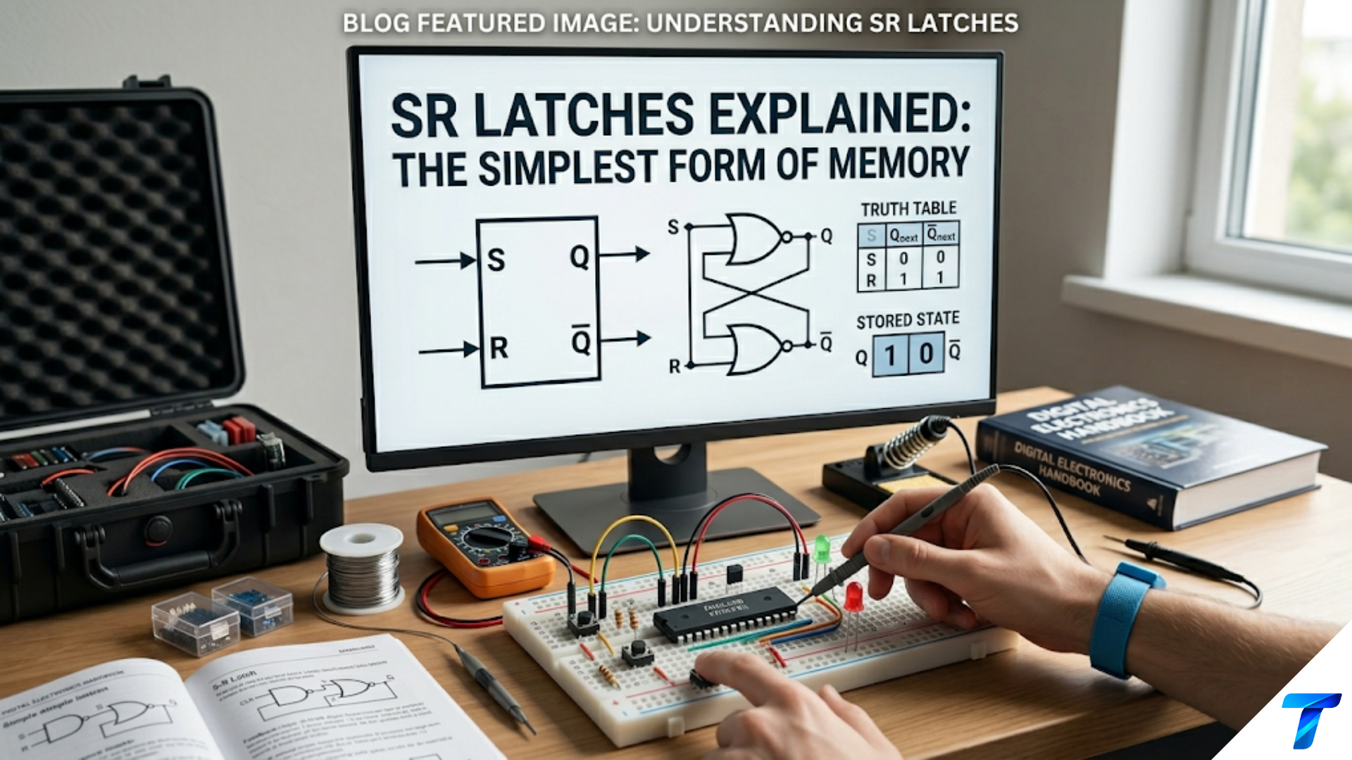
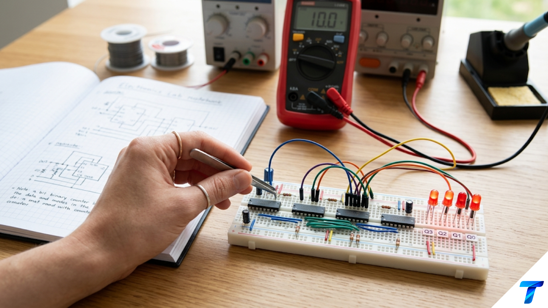
A D flip-flop (Data flip-flop) is an edge-triggered sequential logic circuit that captures the value of its data input (D) at a specific instant — the active edge of a clock signal — and holds that value at its output (Q) until the next active clock edge. Unlike SR latches that respond continuously to inputs, the D flip-flop’s edge triggering means it samples D for only a few nanoseconds per clock cycle, holding Q constant for the entire remaining period. This makes the D flip-flop the universal building block of synchronous digital design, used in registers, pipelines, counters, shift registers, and all sequential logic.
Introduction: The Heartbeat of Synchronous Logic
Every modern digital system operates synchronously — its state changes happen at precise, predictable moments defined by a clock signal. This synchronous discipline, where all flip-flops in a system capture their new values simultaneously at the clock edge, is what makes billion-gate digital circuits reliable and analyzable. Without it, with different parts of the circuit changing at different times, the interactions between signals would produce races, hazards, and unpredictable behavior impossible to characterize or debug.
The D flip-flop is the element that makes synchronous design possible and practical. Its single data input D eliminates the forbidden state of the SR latch. Its edge triggering eliminates the transparency problem of the D latch. The result is a memory element with one clean behavioral rule: whatever D is at the moment the clock edge arrives, that is what Q becomes, and Q holds that value steadfastly until the next clock edge regardless of any subsequent changes to D.
This simplicity is deceptive in its power. Chain D flip-flops together and you get shift registers that serialize and deserialize data. Connect a flip-flop’s Q̄ back to D and you get a divide-by-2 frequency divider. Add combinational logic between flip-flop stages and you get finite state machines that implement any sequential behavior. Load parallel data into a bank of flip-flops and you have a register. Connect multiple registers to a shared bus with enable logic and you have a register file — the core of a CPU.
Understanding the D flip-flop thoroughly — not just its truth table but the internal mechanism that creates edge triggering, the critical timing parameters and what violations mean, the metastability phenomenon and how to manage it, and the design patterns that use D flip-flops — is arguably the most important single topic in digital electronics after Boolean algebra itself. This article provides that complete understanding.
Internal Structure: How Edge Triggering Is Achieved
The Fundamental Challenge
A latch is transparent while its enable is HIGH — Q tracks D continuously during the enable period. This creates a problem: if the latch’s own Q output feeds back through logic to influence D (as happens in counters and state machines), the circuit may race through multiple states during a single enable pulse rather than advancing exactly one state per clock cycle.
The solution requires that the flip-flop capture D for only a single instant — ideally zero duration — at the clock edge, not during the entire clock half-cycle. No real circuit can capture data in zero time, but the master-slave configuration achieves the next best thing: it captures data during the first half of the clock cycle (in the master latch) and transfers it to the output during the second half (in the slave latch). The output Q is isolated from the input D for the entire duration of one clock phase, preventing feedback races.
Master-Slave D Flip-Flop Construction
The positive-edge-triggered D flip-flop uses two cascaded D latches with complementary clock enables:
Master latch: Enable = CLK̄ (inverted clock)
- Transparent when CLK=0: Master captures and tracks D
- Latched when CLK=1: Master holds whatever D was when CLK rose
Slave latch: Enable = CLK
- Latched when CLK=0: Slave holds previous Q value, isolated from master
- Transparent when CLK=1: Slave captures master’s held value, Q updates
Data flow through one complete clock cycle:
Phase 1 (CLK=0):
- Master enable = CLK̄ = 1 → Master is TRANSPARENT, tracks D continuously
- Slave enable = CLK = 0 → Slave is LATCHED, Q holds previous value
Transition (CLK: 0→1, the positive edge):
- Master enable = CLK̄ transitions 1→0: Master LATCHES at the moment CLK rises
- Slave enable = CLK transitions 0→1: Slave becomes TRANSPARENT at the same moment
Phase 2 (CLK=1):
- Master is LATCHED: holds value D had at the clock’s rising edge
- Slave is TRANSPARENT: immediately captures master’s held value → Q updates
Phase 3 (CLK: 1→0, the negative edge):
- Master enable = CLK̄ transitions 0→1: Master becomes transparent again
- Slave enable = CLK transitions 1→0: Slave latches, Q holds until next rising edge
The key insight: Q updates at the positive clock edge (CLK: 0→1) and holds stable throughout CLK=1 and all of CLK=0 until the next positive edge. D can change freely during CLK=1 and CLK=0 with no effect on Q — the slave is latched during both these periods. Only the state of D at the instant of the positive edge matters.
Why This Prevents Feedback Races
In a synchronous counter where Q feeds back through logic to D:
With a D latch (CLK=enable): When CLK=1, Q drives D through logic. Since the latch is transparent, Q immediately reflects D, which changes Q again — the circuit races through multiple states.
With a master-slave D flip-flop:
- During CLK=0: Master updates (tracking D through feedback from Q). But slave is latched — Q is stable. The feedback from Q remains constant, so D is stable. Master correctly captures the intended next state.
- At CLK rising edge: Master latches, slave becomes transparent. Q updates to the master’s held value. This changes D through feedback — but master is now latched and cannot respond until CLK falls again. One state transition per clock cycle, guaranteed.
This isolation of Q from D during each clock phase is what synchronous design depends on.
CMOS Transmission Gate Implementation
Modern CMOS D flip-flops use transmission gates (pass transistors) rather than gated NAND/NOR latches for lower power, higher speed, and smaller area:
A CMOS D latch uses two transmission gates (a series NMOS-PMOS pair that either passes or blocks a signal) with complementary enable:
When EN=1: TG1 conducts (passes D to the inverter chain), TG2 is open (breaks feedback). The latch is transparent — D propagates to Q through two inverters.
When EN=0: TG1 is open (blocks D), TG2 conducts (closes the feedback loop around the two inverters). The latch is closed — Q is held by the cross-coupled inverter pair.
Two such transmission-gate latches in master-slave configuration form a D flip-flop in as few as 8 transistors — the minimum for any flip-flop. Commercial flip-flop cells in advanced CMOS processes use approximately 12–20 transistors for a complete D flip-flop with Q̄ output, balanced drive strength, and power optimizations.
D Flip-Flop Timing: The Parameters That Matter
Setup Time (t_su): The Advance Notice Requirement
The setup time is the minimum duration that D must be stable before the active clock edge. The flip-flop needs this window to propagate D through its internal logic (particularly the master latch) far enough that the captured value is unambiguous before the clock edge locks the master.
D must be stable for at least t_su BEFORE the clock edgeWhat violates setup time: D changing within the t_su window before the clock edge. If D is still transitioning — neither a clean 0 nor a clean 1 — when the clock edge arrives, the master latch may capture an ambiguous intermediate voltage.
Typical values (74HC74 at 5V): t_su = 5ns
Implication for system design: The combinational logic that generates D must complete its propagation at least t_su before the clock edge. The constraint:
t_pCLK-Q (previous flip-flop) + t_logic (combinational path) ≤ T_clock - t_suWhere T_clock is the clock period. Rearranging for maximum clock frequency:
f_max = 1 / (t_pCLK-Q + t_logic + t_su)Hold Time (t_h): The Stability Window After the Edge
The hold time is the minimum duration that D must remain stable AFTER the active clock edge. The flip-flop continues reading D for a brief period after the clock edge while the internal transmission gates finish switching and the feedback loop closes.
D must remain stable for at least t_h AFTER the clock edgeWhat violates hold time: D changing within t_h after the clock edge — this can corrupt the just-captured value before it is fully stored.
Typical values (74HC74 at 5V): t_h = 5ns
Hold time violations are particularly dangerous because they depend on the propagation delay from the driving flip-flop to the receiving flip-flop. If the path between two flip-flops is very short (fast, direct connection), the new D value from the driving flip-flop may arrive at the receiving flip-flop’s D input before t_h has elapsed after the common clock edge. Unlike setup time violations (which can be fixed by slowing the clock or shortening logic paths), hold time violations cannot be fixed by changing the clock frequency — they require adding delay in the data path.
Hold time margin:
t_hold_margin = t_pCLK-Q_driver + t_logic_path - t_h_receiverThis must be ≥ 0. If negative, a hold time violation exists regardless of clock frequency.
Propagation Delay (t_pCLK-Q): From Edge to Output
The time from the active clock edge to when Q reaches a valid new logic level:
t_pCLK-Q: delay from CLK↑ to valid Q outputTypical values (74HC74 at 5V): t_pCLK-Q = 14ns maximum
There are actually two specified values:
- t_pCLK-Q(H): Time for Q to transition LOW→HIGH (rising)
- t_pCLK-Q(L): Time for Q to transition HIGH→LOW (falling)
These may differ slightly due to PMOS vs. NMOS drive strength asymmetry. The larger of the two is the critical value for timing analysis.
Asynchronous Input Timing (t_pPRE-Q, t_pCLR-Q)
The PRE̅ and CLR̅ asynchronous inputs have their own propagation delays — from assertion of PRE̅ or CLR̅ to the resulting Q output change:
74HC74: t_pPRE-Q and t_pCLR-Q = 16ns maximum at 5V
These are slightly longer than the clock-to-Q delay because the asynchronous path propagates through additional gate levels inside the flip-flop.
Recovery time (t_rec): PRE̅ and CLR̅ must be released (go HIGH) at least t_rec before the next active clock edge to avoid interfering with clocked operation. The flip-flop’s internal logic must clear the asynchronous override before the clock arrives.
74HC74: t_rec = 5ns
If PRE̅ or CLR̅ is still asserted within t_rec of the clock edge, the clock-controlled D capture and the asynchronous override compete, potentially causing metastability.
Timing Parameter Summary Table
| Parameter | Symbol | 74HC74 @ 5V | Meaning |
|---|---|---|---|
| Setup time | t_su | 5ns | D stable before CLK↑ |
| Hold time | t_h | 5ns | D stable after CLK↑ |
| Clock-to-Q delay | t_pCLK-Q | 14ns max | CLK↑ to valid Q |
| PRE/CLR-to-Q delay | t_pPRE-Q | 16ns max | Async set/reset to Q |
| Recovery time | t_rec | 5ns | PRE/CLR release before CLK |
| Min clock pulse width | t_W(H), t_W(L) | 10ns | CLK high/low duration |
| Max clock frequency | f_max | ~50MHz | 1/(t_pCLK-Q + t_su) @ no logic |
Metastability in D Flip-Flops
When Timing Violations Occur
Despite careful synchronous design, situations exist where D inevitably changes near the clock edge:
- Asynchronous inputs: A button press, external interrupt, or data from a different clock domain arrives at an unpredictable time relative to the local clock
- Clock domain crossings: Data generated by one clock must be read by a different clock — the two clocks have no phase relationship
- Test and debug: Manual clock stepping or probe-induced delays
When D changes within the setup-hold window around the clock edge, the flip-flop may enter a metastable state.
The Physics of Metastability
The D flip-flop’s internal storage element is a bistable circuit (cross-coupled inverters or transmission gates forming a regenerative loop) with an unstable equilibrium at V_DD/2. When the clock edge arrives while D is near this equilibrium, the storage node may be captured at an intermediate voltage.
The flip-flop’s regenerative loop then drives the stored voltage toward one of the two stable rails (0 or V_DD) exponentially:
V(t) = V_meta × exp(t / τ)Where V_meta is the initial deviation from the metastable point and τ is the regeneration time constant (related to the transistor’s gain-bandwidth product). The signal grows exponentially — but starting from a very small initial value, it may take many time constants to reach a valid logic level.
The resolution time problem: Unlike setup/hold violations that cause definite wrong values, metastability produces output at an uncertain voltage for an uncertain duration. The output may:
- Resolve quickly (within 1 clock cycle) to a correct or incorrect value
- Linger at intermediate voltage for multiple clock cycles
- Even oscillate in rare cases
Statistical characterization:
P(metastable after t_resolve) = f_data × f_clk × T_meta × exp(-t_resolve / τ)Where f_data is the rate of asynchronous input events, f_clk is the clock frequency, T_meta is a device-specific metastability window parameter, and τ is the regeneration constant.
For 74HC74 at 5V: τ ≈ 0.5ns. After t_resolve = 10ns: exp(-10/0.5) = exp(-20) ≈ 2×10⁻⁹ — very small probability.
Managing Metastability: The Two-Flop Synchronizer
The standard solution for crossing from an asynchronous or different-clock-domain signal into a synchronous domain is a two-stage synchronizer:
Stage 1: First D flip-flop samples the asynchronous input. This flip-flop may go metastable.
Stage 2: Second D flip-flop samples the first flip-flop’s output one clock cycle later.
Between Stage 1’s clock edge and Stage 2’s clock edge is one full clock period (say 10ns at 100MHz). This is the resolution time allowed for Stage 1’s metastability to resolve. If Stage 1’s output has not resolved to a valid logic level within this window, Stage 2 will see an invalid voltage and may also go metastable.
The probability that BOTH flip-flops are metastable after one clock period is:
P_both_metastable ≈ [P_stage1_metastable(T_clk)]² This is exponentially smaller than a single flip-flop’s metastability probability. Adding a third stage reduces it further by another exponential factor.
Typical result: A well-designed two-flop synchronizer at 100MHz with modern CMOS processes achieves MTBF (Mean Time Between Failures due to metastability) measured in thousands to millions of years — acceptable for all practical applications.
Three-flop synchronizer: For very high clock frequencies (>500MHz) where the clock period provides insufficient resolution time, three flip-flops in series provide a full two clock periods for metastability resolution.
D Flip-Flop Applications: The Building Blocks of Sequential Systems
Pattern 1: Simple Data Register
A single D flip-flop stores one bit. Its clock input (LOAD or WRITE_ENABLE) captures D when pulsed.
For N bits, use N flip-flops sharing a common clock. The 74HC74 (2 flip-flops), 74HC175 (4 flip-flops), 74HC273 (8 flip-flops) package multiple flip-flops for byte-wide and word-wide registers.
Key property: All bits capture simultaneously — the propagation delay from CLK to any Q output is the same t_pCLK-Q. No inter-bit skew in a well-designed IC.
Pattern 2: Pipeline Register
A pipeline register sits between two stages of combinational logic, allowing both stages to operate simultaneously on different data:
Input → [Stage 1 Logic] → [Pipeline Register] → [Stage 2 Logic] → OutputWithout pipelining: a computation taking 20ns of logic delay limits throughput to 1 operation per 20ns.
With pipelining: while Stage 1 computes new data, Stage 2 processes the data Stage 1 computed in the previous cycle. Both stages are busy simultaneously. Throughput doubles (1 operation per 10ns), though latency increases (the result takes two clock cycles to emerge).
Modern processors use 10–20 pipeline stages, each separated by D flip-flop registers. An instruction takes 10–20 clock cycles from fetch to retirement (latency), but the processor completes one instruction per clock cycle (throughput) because 10–20 instructions are in flight simultaneously.
Pattern 3: Synchronizer for Asynchronous Input
As described in the metastability section: two D flip-flops in series, sharing the system clock, with the asynchronous signal at the first flip-flop’s D input. The synchronized output from the second flip-flop is safe to use in the synchronous domain.
ASYNC_IN → [FF1] → [FF2] → SYNC_OUT
            CLK     CLK
Critical rule: never use FF1’s Q output directly — always use FF2’s Q. The one-clock-cycle delay between FF1 and FF2 is mandatory for metastability resolution.
Pattern 4: Frequency Divider
Connect Q̄ to D (feedback). On each positive clock edge:
- If Q=0: D=Q̄=1 → Q captures 1, becomes 1
- If Q=1: D=Q̄=0 → Q captures 0, becomes 0
Q toggles on every clock edge, producing output at half the clock frequency. Three flip-flops in series divide by 8; N flip-flops divide by 2^N.
Pattern 5: Shift Register
N flip-flops in series, each one’s Q feeding the next one’s D, all sharing a common clock:
SER_IN → [FF0] → [FF1] → [FF2] → [FF3] → PARALLEL_OUT (Q0-Q3)
          CLK     CLK     CLK     CLK
On each clock edge, each bit shifts one position to the right. After 4 clocks, 4 serial bits appear simultaneously on Q0-Q3. This is serial-to-parallel conversion.
Running the same register in reverse (Q3 as output, data fed in at FF3’s D) gives parallel-to-serial conversion.
Pattern 6: Synchronous Counter
A D flip-flop with logic between Q and D (combinational feedback) implements a state machine. For a simple 2-bit synchronous up-counter:
Current state: Q1Q0 Next state: Q1_next Q0_next
From the 2-bit counter truth table:
Q0_next = ̄Q0          (Q0 toggles every cycle)
Q1_next = Q1 ⊕ Q0 (Q1 toggles when Q0=1)Gate implementation:
- FF0: D0 = Q̄0 (invert Q0 back to D0)
- FF1: D1 = Q1 ⊕ Q0 (XOR gate on Q1 and Q0)
- Both FFs share common CLK
This advances through: 00 → 01 → 10 → 11 → 00 → … ✓
Pattern 7: Finite State Machine (FSM)
A finite state machine consists of:
- State registers: N flip-flops encoding the current state (2^N possible states)
- Next-state logic: combinational logic computing the next state from current state + inputs
- Output logic: combinational logic computing outputs from current state (and sometimes inputs)
D flip-flops hold the current state. At each clock edge, the next state (computed by combinational logic) is captured. The separation between state memory (flip-flops) and state transition logic (combinational) is the defining structure of synchronous FSM design.
Complete Design Examples
Design Example 1: 4-Bit Parallel Load Register with Read-Back
Application: Store a 4-bit value loaded from an 8-bit data bus (lower nibble), with read-back capability to verify the stored value.
Components:
- 2× 74HC74 (dual D flip-flop) — provides four flip-flops total
- 1× 74HC125 (quad tri-state buffer) — gates the read-back onto the bus
- LOAD signal: positive edge loads D3-D0
- OE̅ signal: active-LOW enables Q3-Q0 onto the bus
Connections:
74HC74 #1:
  FF0: D0=BUS0, CLK=LOAD, PRE̅=1, CLR̅=RESET̅, Q0=internal + tri-state buffer input
  FF1: D1=BUS1, CLK=LOAD, PRE̅=1, CLR̅=RESET̅, Q1=internal + tri-state buffer input

74HC74 #2:
  FF2: D2=BUS2, CLK=LOAD, PRE̅=1, CLR̅=RESET̅, Q2=internal + tri-state buffer input
  FF3: D3=BUS3, CLK=LOAD, PRE̅=1, CLR̅=RESET̅, Q3=internal + tri-state buffer input

74HC125 #1 (four buffers):
Buffer i: input=Qi, OE̅=READ̅, output→BUS_iOperation:
- Place data on BUS3-BUS0
- Assert LOAD (rising edge) — all four FFs capture simultaneously
- Release LOAD — FFs hold data independently of bus changes
- To read back: assert READ̅ (LOW) — Q3-Q0 drive the bus through tri-state buffers
- Release READ̅ — buffers go high-impedance, releasing the bus
Timing requirements:
- BUS must be stable for t_su=5ns before LOAD rising edge
- BUS must remain stable for t_h=5ns after LOAD rising edge
- LOAD pulse must be ≥ t_W(H)=10ns wide
Reset: Assert RESET̅=LOW — all Q outputs immediately go LOW (asynchronous, independent of clock).
Design Example 2: 8-Bit Serial-In Parallel-Out Shift Register
Application: Receive 8 bits serially (one bit per clock cycle, MSB first) and present them simultaneously on 8 output lines after 8 clocks.
Components:
- 4× 74HC74 (8 flip-flops total: 4 ICs × 2 FFs each)
- SHIFT_CLK: shared clock input
- SERIAL_IN: first flip-flop data input
- PARALLEL_OUT: Q7-Q0 (all eight Q outputs)
Connections:
FF0: D=SERIAL_IN, CLK=SHIFT_CLK, Q=D_FF1 and Q0_OUT
FF1: D=Q0, CLK=SHIFT_CLK, Q=D_FF2 and Q1_OUT
FF2: D=Q1, CLK=SHIFT_CLK, Q=D_FF3 and Q2_OUT
FF3: D=Q2, CLK=SHIFT_CLK, Q=D_FF4 and Q3_OUT
FF4: D=Q3, CLK=SHIFT_CLK, Q=D_FF5 and Q4_OUT
FF5: D=Q4, CLK=SHIFT_CLK, Q=D_FF6 and Q5_OUT
FF6: D=Q5, CLK=SHIFT_CLK, Q=D_FF7 and Q6_OUT
FF7: D=Q6, CLK=SHIFT_CLK, Q=Q7_OUTTiming walkthrough — shifting in byte 0b10110001 (MSB first: 1,0,1,1,0,0,0,1):
| Clock | SERIAL_IN | Q7 | Q6 | Q5 | Q4 | Q3 | Q2 | Q1 | Q0 |
|---|---|---|---|---|---|---|---|---|---|
| 0 | — | 0 | 0 | 0 | 0 | 0 | 0 | 0 | 0 |
| ↑1 | 1 | 0 | 0 | 0 | 0 | 0 | 0 | 0 | 1 |
| ↑2 | 0 | 0 | 0 | 0 | 0 | 0 | 0 | 1 | 0 |
| ↑3 | 1 | 0 | 0 | 0 | 0 | 0 | 1 | 0 | 1 |
| ↑4 | 1 | 0 | 0 | 0 | 0 | 1 | 0 | 1 | 1 |
| ↑5 | 0 | 0 | 0 | 0 | 1 | 0 | 1 | 1 | 0 |
| ↑6 | 0 | 0 | 0 | 1 | 0 | 1 | 1 | 0 | 0 |
| ↑7 | 0 | 0 | 1 | 0 | 1 | 1 | 0 | 0 | 0 |
| ↑8 | 1 | 1 | 0 | 1 | 1 | 0 | 0 | 0 | 1 |
After 8 clocks, Q7-Q0 = 10110001 = the transmitted byte ✓
Key insight: All eight flip-flops shift simultaneously on each clock edge. The shift happens because each D input sees the previous Q output — which was the value from one clock ago. Since all Q outputs update simultaneously at the clock edge, each FF captures its neighbor’s pre-edge value, creating a coordinated shift.
Maximum shift frequency: With 74HC74 (t_pCLK-Q=14ns, t_su=5ns, t_h=5ns, zero logic delay between stages):
f_max = 1 / (t_pCLK-Q + t_h) = 1 / (14ns + 5ns) = 1 / 19ns ≈ 52MHzActually for shift register timing, the critical path is hold time (D of FF1 changes 14ns after the clock edge due to FF0’s propagation delay; hold time of FF1 requires D stable for only 5ns after the edge — since 14ns > 5ns, hold time is met with 9ns margin).
Setup time check: Next clock can arrive as soon as t_pCLK-Q + 0 (no logic) + t_su = 14+5=19ns after current clock → f_max = 52MHz ✓
Real-world implementation: The 74HC595 (serial-in, parallel-out with storage register) handles this in a single 16-pin IC with the added benefit of a separate storage latch that holds the parallel outputs stable while new data is being shifted in.
Design Example 3: Two-Flop Synchronizer for Button Input
Application: A button connected to an FPGA or microcontroller running at 50MHz. The button is entirely asynchronous — it may be pressed at any time relative to the 50MHz clock. Implement a reliable synchronizer that outputs a clean, synchronized version of the button state.
Components (discrete implementation):
- 1× 74HC74 (dual D flip-flop — uses both FFs)
- 10kΩ pull-up resistor on button
- 10nF filter capacitor (optional RC filter for additional noise suppression)
Circuit:
VCC ──[10kΩ]──┬──── BUTTON_RAW
              │
BUTTON ────  GND (when pressed)
              │
       [10nF cap to GND] (optional RC filter)
              │
BUTTON_RAW ──→ D1 (pin 2 of 74HC74)
CLK_50MHz ──→ CLK1 (pin 3 of 74HC74)
PRE̅1 (pin 4) ── VCC
CLR̅1 (pin 1) ── VCC

Q1 (pin 5) ──→ D2 (pin 12 of 74HC74)
CLK_50MHz ──→ CLK2 (pin 11 of 74HC74)
PRE̅2 (pin 10) ── VCC
CLR̅2 (pin 13) ── VCC

Q2 (pin 9) ──→ BUTTON_SYNC (synchronized output — USE THIS)
Q1 (pin 5) ──→ DO NOT USE DIRECTLYTiming analysis:
- Clock period T = 20ns (50MHz)
- FF1 may go metastable when button pressed
- FF2 samples FF1’s output 20ns later
- 20ns resolution time for FF1’s metastability: P(still metastable) = exp(-20/0.5) ≈ 10⁻¹⁷
With button press rate of 10Hz and clock at 50MHz:
MTBF = 1 / (f_data × f_clk × T_meta × exp(-T_clk/τ))
≈ 1 / (10 × 50×10⁶ × T_meta × 10⁻¹⁷)Even with T_meta = 1ns (pessimistic): MTBF ≈ 1/(10 × 5×10⁷ × 10⁻⁹ × 10⁻¹⁷) = 2×10¹⁸ seconds — effectively infinite. ✓
Edge detection (optional — produces one-cycle pulse on button press): Add one gate: PRESS_PULSE = Q2 AND ̄Q2_delayed Where Q2_delayed is Q2 one clock cycle earlier (a third flip-flop: D=Q2, CLK=same clock):
PRESS_PULSE = Q2 · ̄Q2_prevOne gate from 74HC08 and half of a third 74HC74 for the delay flip-flop.
Design Example 4: 2-Bit Synchronous Up/Down Counter
Application: Count up or down on each clock edge based on a UP/DOWN̄ control signal. Count sequence: 00→01→10→11→00 (up) or 00→11→10→01→00 (down). LEDs display current count.
State transition table:
| Current Q1Q0 | UP/DOWN̄=1 (up) next | UP/DOWN̄=0 (down) next |
|---|---|---|
| 00 | 01 | 11 |
| 01 | 10 | 00 |
| 10 | 11 | 01 |
| 11 | 00 | 10 |
Next-state logic derivation:
For Q0_next (using K-map with variables Q1, Q0, U where U = UP/DOWN̄):
| U | Q1Q0=00 | Q1Q0=01 | Q1Q0=11 | Q1Q0=10 |
|---|---|---|---|---|
| 0 | 1 | 0 | 0 | 1 |
| 1 | 1 | 0 | 0 | 1 |
Q0_next is independent of U! Looking at the pattern: Q0_next = ̄Q0 (Q0 toggles every cycle for both up and down counting).
For Q1_next:
| U | Q1Q0=00 | Q1Q0=01 | Q1Q0=11 | Q1Q0=10 |
|---|---|---|---|---|
| 0 | 1 | 1 | 0 | 0 |
| 1 | 0 | 1 | 1 | 0 |
Wait — let me re-derive from the table:
- When U=1 (up): 00→01, 01→10, 10→11, 11→00 Q1_next: 0,1,1,0 → Q1_next = Q1 ⊕ Q0 for up count
- When U=0 (down): 00→11, 01→00, 10→01, 11→10 Q1_next: 1,0,0,1 → for 00: Q1_next=1; for 01: Q1_next=0; for 10: Q1_next=0; for 11: Q1_next=1
Hmm let me redo the up-case Q1_next:
- 00→01: Q1_next=0 ✓
- 01→10: Q1_next=1 ✓
- 10→11: Q1_next=1 ✓
- 11→00: Q1_next=0 ✓
Q1_next (up) = Q1 ⊕ Q0? Check: 00: 0⊕0=0✓, 01: 0⊕1=1✓, 10: 1⊕0=1✓, 11: 1⊕1=0✓ ✓
Down case Q1_next:
- 00→11: Q1_next=1
- 01→00: Q1_next=0
- 10→01: Q1_next=0
- 11→10: Q1_next=1
Q1_next (down) = Q1 ⊕ Q̄0? Check: 00: 0⊕1=1✓, 01: 0⊕0=0✓, 10: 1⊕1=0✓… wait 10→01 gives Q1_next=0. 1⊕Q̄0=1⊕(̄0)=1⊕1=0… Q̄0 for Q0=0 is 1. So 1⊕1=0. But we need Q1_next=0 for 10 case. 1⊕1=0 ✓. For 11: 1⊕0=1 ✓.
Q1_next = Q1 ⊕ Q̄0 for down count.
Unified expression using multiplexer (U selects Q0 or Q̄0 as the XOR operand):
Q1_next = Q1 ⊕ (U·Q0 + Ū·Q̄0)
= Q1 ⊕ (Q0 XNOR U)Let’s verify:
- U=1 (up): Q0 XNOR 1 = Q0 ⊕ 1 ⊕ … wait, XNOR(Q0, U=1) = ̄(Q0⊕1) = ̄Q̄0 = Q0. So Q1_next = Q1 ⊕ Q0 ✓
- U=0 (down): XNOR(Q0, U=0) = ̄(Q0⊕0) = ̄Q0 = Q̄0. So Q1_next = Q1 ⊕ Q̄0 ✓
Gate implementation:
Gate 1 (NOT): Q0 → Q̄0
Gate 2 (XNOR or XOR+NOT): Q0 and U → (Q0 XNOR U) = TEMP1
  XNOR(Q0, U) = ̄(Q0⊕U): one XOR gate + one NOT gate, or use one 74HC266/74HC7266
  Alternative: XNOR(Q0,U) = Q0·U + Q̄0·Ū = two ANDs + one OR + one NOT

Gate 3 (XOR): Q1 and TEMP1 → D1 = Q1_next
Gate 4 (NOT): Q0 → D0 = Q̄0 = Q0_nextFull circuit:
- 2× 74HC74 flip-flops (one per bit, both on one IC)
- 1× 74HC86 (XOR for Q1_next part and for XNOR together)
- 1× 74HC08 (AND) + 74HC32 (OR) if using AND/OR for XNOR, OR simply use 74HC7266 XNOR
Simpler: use two XOR gates and one NOT:
TEMP = Q0 XOR U        [one 74HC86 gate]
D1 = Q1 XOR TEMP = Q1 XOR Q0 XOR U  [second 74HC86 gate]

Wait: Q1 XOR (Q0 XOR U):
- U=1: Q1 XOR Q0 XOR 1 = ̄(Q1 XOR Q0)... that's not what we want.Rechecking: We need D1 = Q1 ⊕ XNOR(Q0, U) = Q1 ⊕ ̄(Q0 ⊕ U).
Let TEMP = Q0 ⊕ U (XOR gate). TEMP̄ = ̄(Q0 ⊕ U) = XNOR(Q0, U) (NOT gate on TEMP). D1 = Q1 ⊕ TEMP̄ (XOR gate).
Final gate count: 1 XOR (TEMP) + 1 NOT (TEMP̄) + 1 XOR (D1) + 1 NOT (D0=Q̄0) = 2 XOR + 2 NOT gates.
ICs: 74HC74 (both FFs for Q0, Q1) + 74HC86 (two XOR gates) + 74HC04 (two NOT gates). Three ICs total.
Verification — count up from 00:
- Q1=0, Q0=0, U=1: TEMP = 0⊕1 = 1; TEMP̄ = 0; D1 = 0⊕0 = 0; D0 = ̄0 = 1 → next = Q1Q0 = 01 ✓
- Q1=0, Q0=1, U=1: TEMP = 1⊕1 = 0; TEMP̄ = 1; D1 = 0⊕1 = 1; D0 = ̄1 = 0 → next = 10 ✓
- Q1=1, Q0=0, U=1: TEMP = 0⊕1 = 1; TEMP̄ = 0; D1 = 1⊕0 = 1; D0 = ̄0 = 1 → next = 11 ✓
- Q1=1, Q0=1, U=1: TEMP = 1⊕1 = 0; TEMP̄ = 1; D1 = 1⊕1 = 0; D0 = ̄1 = 0 → next = 00 ✓
Count up sequence: 00→01→10→11→00 ✓
Design Example 5: Moore FSM — Sequence Detector
Application: Detect the sequence “101” in a serial bit stream. Output DETECT=1 for exactly one clock cycle when the pattern is recognized. Reset the search after detection (non-overlapping detection).
State diagram:
RESET → S0 (idle, waiting for 1)
S0 + input=1 → S1 (received "1")
S0 + input=0 → S0 (stay idle)
S1 + input=0 → S2 (received "10")
S1 + input=1 → S1 (received another "1", stay)
S2 + input=1 → S3 (received "101" — DETECT here)
S2 + input=0 → S0 (broken sequence, restart)
S3 + input=X → S0 (after detection, reset to idle)Four states: S0=00, S1=01, S2=10, S3=11 (2 flip-flops needed).
State encoding:
- S0: Q1Q0 = 00
- S1: Q1Q0 = 01
- S2: Q1Q0 = 10
- S3: Q1Q0 = 11
Next-state table:
| Current Q1Q0 | Input=0 | Input=1 |
|---|---|---|
| S0 (00) | 00 | 01 |
| S1 (01) | 10 | 01 |
| S2 (10) | 00 | 11 |
| S3 (11) | 00 | 00 |
Output table (Moore — output depends only on current state):
- S0, S1, S2: DETECT=0
- S3: DETECT=1
D1 next-state logic (K-map):
| IN | Q1Q0=00 | Q1Q0=01 | Q1Q0=11 | Q1Q0=10 |
|---|---|---|---|---|
| 0 | 0 | 1 | 0 | 0 |
| 1 | 0 | 0 | 0 | 1 |
D1 is 1 only when: (Q1=0, Q0=1, IN=0) or (Q1=1, Q0=0, IN=1).
D1 = ̄Q1·Q0·̄IN + Q1·̄Q0·IN
= Q0 ⊕ Q1 ... let me verify: Hmm, D1 = Q0·̄IN·̄Q1 + Q1·̄Q0·IN. This is Q0 and Q1 entering two AND gates with IN and its complement:
Group 1: Q1=0, Q0=1, IN=0 → D1=1: term = ̄Q1·Q0·̄IN Group 2: Q1=1, Q0=0, IN=1 → D1=1: term = Q1·̄Q0·IN
D1 = ̄Q1·Q0·̄IN + Q1·̄Q0·IND0 next-state logic:
| IN | Q1Q0=00 | Q1Q0=01 | Q1Q0=11 | Q1Q0=10 |
|---|---|---|---|---|
| 0 | 0 | 0 | 0 | 0 |
| 1 | 1 | 1 | 0 | 0 |
D0=1 when IN=1 AND Q1=0:
D0 = ̄Q1·INOutput logic:
DETECT = Q1·Q0 (S3 state)Gate implementation:
- NOT gate: ̄Q1 (and ̄IN for D1)
- AND gate 1: ̄Q1·Q0·̄IN → D1 term 1 (3-input AND)
- AND gate 2: Q1·̄Q0·IN → D1 term 2 (3-input AND)
- OR gate: D1 terms combined → D1
- AND gate 3: ̄Q1·IN → D0
- AND gate 4: Q1·Q0 → DETECT
ICs: 74HC74 (two FFs), 74HC04 (NOT), 74HC11 (3-input AND for 3-input AND gates), 74HC08 (2-input AND), 74HC32 (OR). Five ICs for this FSM — highlights why programmable logic (GAL, CPLD, FPGA) is preferred over discrete gates for FSMs with more than a few states.
Simulation trace — input sequence 1,1,0,1:
| CLK | IN | Q1Q0 (before) | DETECT | D1 | D0 | Q1Q0 (after) |
|---|---|---|---|---|---|---|
| 1 | 1 | 00 | 0 | 0 | 1 | 01 |
| 2 | 1 | 01 | 0 | 0 | 1 | 01 |
| 3 | 0 | 01 | 0 | 1 | 0 | 10 |
| 4 | 1 | 10 | 0 | 0 | 0 | 11 |
| 5 | — | 11 | 1 | — | — | (detected!) |
After clock 4, the FSM enters state S3 where DETECT=1. ✓ The “101” pattern (received as inputs at clocks 2, 3, 4) is detected.
D Flip-Flop Best Practices in Synchronous Design
Rule 1: All flip-flops share one clock (or one synchronous clock domain)
Connect all flip-flops in a synchronous design to the same clock signal (or to a proper clock tree that distributes the same edge simultaneously to all flip-flops). Mixing different clocks or using asynchronous signals as clocks invites race conditions and metastability.
Rule 2: Never gate the clock
Do not add logic (AND gates, multiplexers) in the clock path to enable or disable flip-flops. Gated clocks introduce clock skew and may create glitches that trigger flip-flops at wrong times. Instead, use clock enable: keep all flip-flops connected to the same clock, but use a D input multiplexer: D = EN·D_new + ̄EN·Q_current. When EN=0, the flip-flop captures its own current value (holds); when EN=1, it captures D_new.
Rule 3: Reset everything to known state
Always connect CLR̅ inputs to a power-on reset circuit. A flip-flop in an unknown state at power-up can cause the system to start in an undefined mode. The power-on reset circuit: VCC through a 10kΩ resistor to a 10µF capacitor whose other end goes to GND. The capacitor keeps CLR̅ (connected to its positive terminal) LOW for ~100ms while charging, then CLR̅ rises HIGH for normal operation.
Rule 4: Minimize clock-to-Q paths through logic
The critical path (longest combinational delay between flip-flop output and next flip-flop input) determines the maximum clock frequency. Keep combinational logic depths shallow. For microcontroller or FPGA targets, use the synthesis tool’s timing report to identify and shorten critical paths.
Rule 5: Check hold time for short paths
Very short paths between flip-flops (direct Q→D connections with no logic, or one gate level) may violate hold time. Calculate: t_pCLK-Q + t_logic ≥ t_h. If this is not satisfied, add a buffer or gate to increase path delay.
Summary
The D flip-flop captures D at the active clock edge and holds Q constant for the entire clock period — a behavior enabled by the master-slave construction where a master latch samples D during one clock phase and a slave latch transfers the captured value to Q during the other phase. This edge triggering eliminates transparency and feedback races, making synchronous design reliable.
Three timing parameters define D flip-flop constraints: setup time (t_su = 5ns for 74HC74 — D must be stable before the edge), hold time (t_h = 5ns — D must be stable after the edge), and propagation delay (t_pCLK-Q = 14ns — Q valid after the edge). Maximum clock frequency = 1/(t_pCLK-Q + t_logic + t_su). Hold time violations require adding delay to short paths, not reducing clock frequency.
Metastability occurs when D changes within the setup-hold window — the flip-flop may linger at an intermediate voltage before resolving. Two-flop synchronizers manage asynchronous inputs by providing one full clock period for metastability resolution, achieving astronomically long MTBF for practical systems.
Seven application patterns — register, pipeline, synchronizer, frequency divider, shift register, counter, and FSM — cover the vast majority of D flip-flop uses. The five design examples demonstrate a 4-bit parallel register, 8-bit shift register (with full timing trace), two-flop synchronizer for button input, 2-bit up/down counter, and a Moore FSM sequence detector. The synchronous design rules — single clock domain, no clock gating, power-on reset, shallow logic paths, hold time checking — provide the framework for reliable system design.