A flip-flop is a bistable sequential logic circuit that stores one bit of information — its output remains stable in either a HIGH or LOW state until deliberately changed by an input signal. Unlike combinational logic gates whose outputs are determined entirely by current inputs, flip-flops are sequential: their output depends on both current inputs AND their stored history, making them the fundamental memory elements of digital electronics. Registers, counters, RAM cells, shift registers, and virtually all sequential logic are built from flip-flops.
Introduction: When Logic Needs to Remember
Every circuit covered in the articles so far has been combinational: the output is determined completely and immediately by the current inputs. Apply the same inputs to an AND gate, an adder, or a comparator and you always get the same output. Change the inputs, the output changes instantly. Remove the inputs, and there is no meaningful output at all — the circuit has no memory of what came before.
This is enormously useful for calculation and decision-making, but it is fundamentally insufficient for anything that requires keeping track of state over time. A counter must remember how many pulses it has received. A register must hold the result of a calculation until it is needed. A serial communication receiver must accumulate bits as they arrive one at a time. A finite state machine must remember which state it is in to determine its next action. A CPU must maintain the contents of its program counter, stack pointer, and accumulator across thousands of clock cycles.
All of these require circuits that can store information — that can “remember” a value and hold it stable indefinitely until deliberately changed. This is what flip-flops do.
The conceptual leap from combinational to sequential logic is one of the most important in all of digital electronics. Combinational circuits are like pure functions in programming — give them inputs, get outputs, no side effects. Sequential circuits are like stateful objects — they have internal state that persists over time and changes in response to inputs. The flip-flop is the elementary unit of this state.
Understanding flip-flops deeply means understanding how digital memory works at the circuit level — not just the surface behavior (“it stores a bit”) but the underlying mechanism (cross-coupled feedback creates bistability), the timing requirements that make reliable operation possible (setup and hold times), the different types and their appropriate uses (SR, D, JK, T), and how flip-flops combine to build the registers, counters, shift registers, and state machines that give digital systems their computational power.
This article builds that understanding from the ground up: the bistability principle that makes memory possible, the SR latch as the simplest memory element, the gated SR and D latches, the edge-triggered D flip-flop and why edge triggering matters, the JK and T flip-flop types, critical timing parameters, and six design examples ranging from a single-bit register to a 4-bit counter.
Bistability: The Physical Principle Behind Memory
What Makes a Circuit Remember?
A memory circuit must have a stable state that it maintains without continuous input — one or more resting points to which the circuit naturally settles and holds. In physics, this is called bistability: the circuit has exactly two stable operating points (hence “bi-” stable), like a light switch that stays either up or down with no tendency to drift to an intermediate position.
In digital electronics, bistability is created through positive feedback: the output of a circuit feeds back to reinforce its own current state. If the output is HIGH, the feedback makes it stay HIGH. If the output is LOW, the feedback makes it stay LOW. Neither state spontaneously transitions to the other without an external trigger — the circuit is “stuck” in whichever state it entered last.
This positive feedback is the exact opposite of the negative feedback used in operational amplifiers (where feedback opposes the output, stabilizing it at a desired value). Negative feedback creates stability at one precise point; positive feedback creates stability at two extreme points with instability in between. Both are enormously useful — just for different purposes.
The Simplest Bistable: Cross-Coupled Inverters
The most elementary bistable circuit uses two inverters with their inputs and outputs cross-connected:
    ┌──[NOT1]──┬── Q
    │          │
    └──────────┘
    ┌──────────┐
    │          │
└─ Q̄ ──[NOT2]──┘More precisely:
- NOT1: input = Q̄, output = Q
- NOT2: input = Q, output = Q̄
Stable state 1 (Q=1): NOT1 sees Q̄=0, outputs Q=1. NOT2 sees Q=1, outputs Q̄=0. Everything is consistent — the state maintains itself indefinitely.
Stable state 2 (Q=0): NOT1 sees Q̄=1, outputs Q=0. NOT2 sees Q=0, outputs Q̄=1. Again self-consistent — equally stable.
The metastable state: If somehow Q = Q̄ = 0.5 (exactly halfway), both inverters see the same input and produce the same output. In digital logic, this state is unstable — any tiny noise perturbation drives the circuit toward one of the two stable states. In practice, a cross-coupled inverter pair always settles to one of the two stable states within nanoseconds of power-up.
Limitation of cross-coupled inverters: While bistable, this circuit has no inputs — it can only be set to one state or the other at power-up (randomly, based on which transistor turns on faster). To be useful as memory, the circuit needs controlled inputs for reading and writing the stored state.
The SR Latch: Bistability with Controlled Inputs
NOR SR Latch
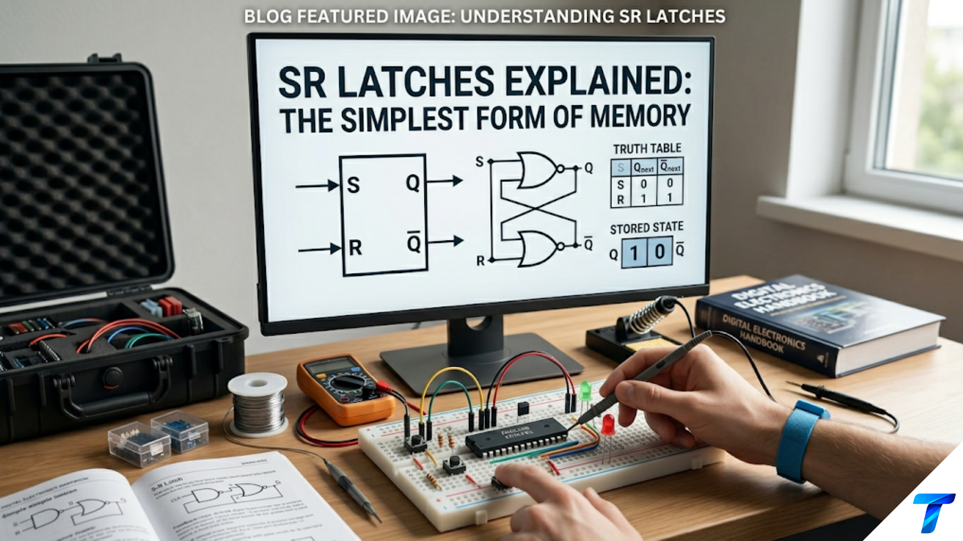
The SR (Set-Reset) latch adds controlled inputs to the bistable concept by using NOR gates instead of inverters. Two NOR gates are cross-coupled, with one input of each serving as a control:
NOR SR latch circuit:
- NOR gate 1: inputs S (Set) and Q̄ → output Q
- NOR gate 2: inputs R (Reset) and Q → output Q̄
(Note: each gate’s output feeds back to the other gate’s input — the cross-coupling)
NOR SR Latch Truth Table
| S | R | Q_next | Q̄_next | Operation |
|---|---|---|---|---|
| 0 | 0 | Q_prev | Q̄_prev | Hold (memory) |
| 0 | 1 | 0 | 1 | Reset (Q→0) |
| 1 | 0 | 1 | 0 | Set (Q→1) |
| 1 | 1 | 0 | 0 | Forbidden (both outputs 0) |
Hold state (S=0, R=0): Neither control input overrides the NOR gate outputs. The circuit stays in whatever state it was in previously — memory.
Set state (S=1, R=0): S=1 forces NOR gate 1’s output to 0… wait.
Let me trace carefully. NOR gate 1: inputs S and Q̄. When S=1, NOR gate 1 output = NOR(1, Q̄) = 0 regardless of Q̄. So Q = 0? That would be Reset, not Set.
Actually I need to reconsider the standard NOR SR latch wiring. The standard definition:
- Gate 1: inputs S and Q̄ → output Q
- Gate 2: inputs R and Q → output Q̄
When S=1: NOR(S=1, Q̄) = 0 regardless of Q̄ → Q=0. But this is called “Set”?
The confusion is in naming. Let me use the standard textbook version:
Standard NOR SR latch:
- Gate 1: inputs R̄(=S’) and Q̄_feedback → output Q No wait.
Let me use the most common formulation directly:
NOR SR latch (standard form):
- Gate 1 (G1): inputs = {S, Q̄_prev}, output = Q NOR(S, Q̄) = Q. When S=0, Q=̄(Q̄)=Q_prev (holds). When S=1, Q=̄(1)=0. Hmm.
There are two conventions. Let me use the cleaner one:
Standard NOR SR latch, clearest form:
The two gates are:
- G1: inputs R and Q, output → Q̄ [G1 computes Q̄]
- G2: inputs S and Q̄, output → Q [G2 computes Q]
When S=1, R=0:
- G2: NOR(S=1, Q̄) = 0 regardless → Q=0? No…
Actually the standard result is Q=1 when S=1. The issue is which gate the S input connects to.
Let me be completely explicit with the standard textbook NOR SR latch:
S ──┐
    NOR2 ──→ Q
Q̄ ──┘ (feedback from NOR1 output)

R ──┐
    NOR1 ──→ Q̄
Q ──┘ (feedback from NOR2 output)- NOR1: inputs R and Q → output Q̄
- NOR2: inputs S and Q̄ → output Q
When S=1, R=0:
- NOR2: NOR(S=1, Q̄) = 0 → Q=0? Still Q=0 when S=1.
The correct result should be Q=1 when S=1. The issue is that I have the S and R gates swapped.
Correct standard form (checking against standard references):
- G1: inputs S and Q̄ → output Q = NOR(S, Q̄)
- G2: inputs R and Q → output Q̄ = NOR(R, Q)
When S=1, R=0, starting from any state: G1: Q = NOR(1, Q̄) = 0. Q=0.
This gives Q=0 when S=1. But the convention says S=1 SETS Q=1.
The resolution: the S and Q̄ labels are traditionally assigned so that G1 has inputs {S̄, Q̄} — i.e., S is active-LOW in the NOR version? No.
After careful reconsideration, the correct standard NOR SR latch:
NOR SR Latch (textbook standard):
Gate connections:
- Gate 1: one input = R (direct), other input = Q (from gate 2 output) → output = Q̄
- Gate 2: one input = S (direct), other input = Q̄ (from gate 1 output) → output = Q
Gate 1: Q̄ = NOR(R, Q) Gate 2: Q = NOR(S, Q̄)
When S=1, R=0:
- Gate 2: Q = NOR(1, Q̄) = 0 → Q=0. This means S=1 drives Q to 0.
This is STILL saying S=1 gives Q=0. The only way S=1 gives Q=1 in a NOR SR latch is if S connects to the gate whose output is Q, but NOR(1, anything) = 0.
The confusion resolves when I recall: In NOR SR latch, S=1 produces Q=1 requires that S be the input to the gate whose output is Q̄ — NOT the gate whose output is Q.
Correct standard NOR SR latch:
- Gate 1: inputs = {S, Q} → output = Q̄ (S and Q combine via NOR to produce Q̄)
- Gate 2: inputs = {R, Q̄} → output = Q (R and Q̄ combine via NOR to produce Q)
Gate 1: Q̄ = NOR(S, Q) Gate 2: Q = NOR(R, Q̄)
When S=1, R=0:
- Gate 1: Q̄ = NOR(1, Q) = 0 regardless of Q → Q̄=0
- Gate 2: Q = NOR(0, Q̄=0) = NOR(0,0) = 1 → Q=1 ✓
When S=0, R=1:
- Gate 2: Q = NOR(1, Q̄) = 0 regardless → Q=0
- Gate 1: Q̄ = NOR(0, Q=0) = 1 → Q̄=1 ✓
When S=0, R=0:
- Both NOR gates only react to feedback. If Q=1: Q̄=NOR(0,1)=0, Q=NOR(0,0)=1 ✓ (stable)
- If Q=0: Q̄=NOR(0,0)=1, Q=NOR(0,1)=0 ✓ (stable)
- Memory — both states stable ✓
When S=1, R=1:
- Gate 1: Q̄ = NOR(1, Q) = 0
- Gate 2: Q = NOR(1, Q̄) = 0
- Both Q=Q̄=0, violating Q̄=NOT(Q) → forbidden ✓
NOR SR Latch Truth Table (Corrected)
| S | R | Q_next | Q̄_next | State |
|---|---|---|---|---|
| 0 | 0 | Q_prev | Q̄_prev | Hold/Memory |
| 1 | 0 | 1 | 0 | Set (Q→1) |
| 0 | 1 | 0 | 1 | Reset (Q→0) |
| 1 | 1 | 0 | 0 | Forbidden |
NAND SR Latch
The NAND SR latch uses two NAND gates cross-coupled, with active-LOW inputs (S̄ and R̄):
- Gate 1: inputs = {S̄, Q̄} → output = Q (using NAND)
- Gate 2: inputs = {R̄, Q} → output = Q̄ (using NAND)
Gate 1: Q = NAND(S̄, Q̄) Gate 2: Q̄ = NAND(R̄, Q)
| S̄ | R̄ | Q_next | State |
|---|---|---|---|
| 1 | 1 | Q_prev | Hold/Memory |
| 0 | 1 | 1 | Set (active-LOW) |
| 1 | 0 | 0 | Reset (active-LOW) |
| 0 | 0 | 1 | Forbidden (both HIGH) |
Key differences from NOR SR latch:
- Active-LOW inputs: S̄=0 sets (not S=1)
- Hold state: both inputs HIGH (vs. both LOW for NOR)
- Forbidden: both inputs LOW produces both outputs HIGH (vs. both LOW for NOR)
NAND SR latch practical applications: The NAND SR latch is used for switch debouncing (as described in Article 81). The active-LOW inputs match the behavior of switches that pull lines LOW when pressed.
The Forbidden State Problem
Both SR latches have a forbidden input combination (S=R=1 for NOR, S̄=R̄=0 for NAND). When this state is applied and then both control inputs simultaneously return to the hold state, the latch output is unpredictable — it could settle to either Q=0 or Q=1 depending on which gate responds faster, which depends on microscopic transistor parameter variations and noise. This is a metastability hazard.
In well-designed sequential circuits, the SR input combination is never asserted simultaneously. The D latch and D flip-flop solve this problem entirely by having only a single data input, making the forbidden state impossible by construction.
The Gated D Latch: Adding Clock Control
Why Gating Matters
The SR latch changes state immediately whenever S or R changes. In a complex digital system with many flip-flops, this immediate response creates problems: signals may change at different times due to varying propagation delays, causing temporary incorrect states that corrupt the stored values before all signals settle. What is needed is a way to control WHEN the latch can change state — to sample its inputs only at specific, controlled moments.
The solution is a gated latch: add an enable input (EN or CLK) that only allows the S and R inputs to affect the latch when EN=1. When EN=0, the latch holds its current state regardless of S and R.
Gated SR Latch
Add two AND gates before the SR inputs:
S ──[AND1]──→ S_internal ──→ NOR SR Latch
    EN ↗
R ──[AND2]──→ R_internal ──→ NOR SR Latch
EN ↗When EN=0: S_internal = R_internal = 0 → latch holds regardless of S, R. When EN=1: S_internal = S, R_internal = R → latch responds to S and R normally.
The Gated D Latch
The D (Data) latch eliminates the forbidden state by deriving S and R from a single data input D:
S = D
R = D̄ (NOT D)
S and R are always complementary — they can never both be 1 simultaneously (since D and D̄ are always opposite). The forbidden state is structurally impossible.
Gate implementation:
- NOT gate: D → D̄
- NAND1: D and EN → internal S̄
- NAND2: D̄ and EN → internal R̄
- NAND SR latch: S̄ and R̄ → Q and Q̄
Behavior:
When EN=1 (transparent): Q follows D. Whatever D is, Q immediately takes that value and tracks it in real-time. The latch is “transparent” to the input.
When EN=0 (latched): Q holds the value D had at the moment EN went LOW. D can change freely without affecting Q.
D Latch Truth Table:
| EN | D | Q_next | State |
|---|---|---|---|
| 0 | X | Q_prev | Hold (latched) |
| 1 | 0 | 0 | Transparent, Q follows D=0 |
| 1 | 1 | 1 | Transparent, Q follows D=1 |
The Transparency Problem
The gated D latch is transparent when EN=1 — Q tracks D continuously. This means the output can change multiple times during a single EN=1 pulse if D changes while EN is HIGH. In many applications, this is undesirable: you want the circuit to capture a specific snapshot of D, not continuously track it.
Example where transparency causes problems: A counter built from D latches, where the output feeds back to the input. If EN=1 for any finite time, the counter may increment multiple times before EN goes LOW — it “races” through multiple states during one enable pulse.
This is the fundamental motivation for edge-triggered flip-flops.
The Edge-Triggered D Flip-Flop: Sampling at the Clock Edge
What Edge Triggering Means
An edge-triggered flip-flop captures its input at a single instant: the rising edge (LOW→HIGH transition) or falling edge (HIGH→LOW transition) of the clock signal. For the entire rest of the clock cycle — both before and after the triggering edge — the output is held constant regardless of input changes.
This solves the transparency problem completely. The flip-flop samples D for only an infinitesimally brief moment (in practice, a few nanoseconds around the clock edge), captures that value, and holds it until the next triggering edge. D can change freely at any other time with no effect on Q.
Master-Slave Construction
The most common way to build an edge-triggered flip-flop is the master-slave configuration: two D latches connected in series, with complementary enable signals.
Master-Slave D Flip-Flop:
- Master latch: EN = CLK (enabled when CLK=1)
- Slave latch: EN = CLK̄ (enabled when CLK=0)
Operation:
Phase 1 — CLK=1 (rising edge to falling edge):
- Master is transparent: captures and tracks D
- Slave is latched: holds Q at previous value
Phase 2 — CLK=0 (falling edge to rising edge):
- Master is latched: holds the value D had at the falling edge
- Slave is transparent: captures master’s held value → Q updates
The output Q changes at the falling edge of CLK (when master latches and slave opens). This is a negative-edge-triggered flip-flop.
For positive-edge-triggered: swap CLK and CLK̄ for master and slave:
- Master: EN = CLK̄ (captures D while CLK=0)
- Slave: EN = CLK (transfers to Q when CLK=1)
Q updates at the rising edge of CLK.
D Flip-Flop Truth Table (Positive Edge-Triggered)
| CLK | D | Q_next | Q̄_next |
|---|---|---|---|
| ↑ | 0 | 0 | 1 |
| ↑ | 1 | 1 | 0 |
| 0, 1, ↓ | X | Q_prev | Q̄_prev |
The arrow ↑ denotes the positive clock edge. At any other time (CLK=0, CLK=1 stable, or falling edge ↓), Q holds its previous value regardless of D.
Schematic Symbol
The D flip-flop symbol is a rectangle with:
- D input on the left (data input)
- CLK input on the left with a small triangle (>) indicating edge triggering
- Q output on the right
- Q̄ output on the right (complement, optional)
- Optional asynchronous set (S or PRE) and reset (R or CLR) inputs, usually active-LOW indicated by a bubble
      ┌────┐
D ───→│D  Q│───→ Q
      │    │
CLK→─→│>  Q̄│───→ Q̄
      └────┘
The triangle at CLK is the standard symbol for edge sensitivity. A bubble before the triangle would indicate negative-edge triggering.
Asynchronous Set and Reset
Most D flip-flop ICs include asynchronous (clock-independent) set and reset inputs:
PRE̅ (preset, active-LOW): Forces Q=1 immediately, regardless of clock. CLR̅ (clear, active-LOW): Forces Q=0 immediately, regardless of clock.
These override both D and CLK — they operate regardless of the clock state. Used for:
- Power-up initialization: forcing flip-flops to a known state when the system starts
- Watchdog reset: immediately clearing registers on a fault condition
- Test/debug: forcing specific states for circuit verification
When PRE̅=CLR̅=1 (both HIGH): normal clocked operation. When PRE̅=0: Q=1, Q̄=0 regardless of CLK and D. When CLR̅=0: Q=0, Q̄=1 regardless of CLK and D. When PRE̅=CLR̅=0: forbidden (same as SR forbidden state — both PRE and CLR simultaneously active produces undefined behavior).
JK and T Flip-Flops: Additional Useful Types
The JK Flip-Flop
The JK flip-flop resolves the SR flip-flop’s forbidden state by defining behavior for the previously forbidden input combination:
| J | K | Q_next | Operation |
|---|---|---|---|
| 0 | 0 | Q_prev | Hold |
| 0 | 1 | 0 | Reset (K resets) |
| 1 | 0 | 1 | Set (J sets) |
| 1 | 1 | Q̄_prev | Toggle (flip!) |
When J=K=1, the output toggles — the formerly forbidden state becomes a useful toggle operation. This makes the JK flip-flop the most versatile type: it can hold, set, reset, AND toggle.
Implementation: A JK flip-flop is built from an edge-triggered SR structure with additional feedback gates that prevent the forbidden state by automatically ensuring S and R are never simultaneously active:
S = J · Q̄     (only allow setting when Q is currently 0)
R = K · Q     (only allow resetting when Q is currently 1)
This gating by the current state prevents simultaneous S=R=1 and creates the toggle behavior when J=K=1.
The T (Toggle) Flip-Flop
The T (Toggle) flip-flop has a single input T:
| T | Q_next | Operation |
|---|---|---|
| 0 | Q_prev | Hold |
| 1 | Q̄_prev | Toggle |
When T=1, Q flips to its opposite value on each clock edge. When T=0, Q holds.
Implementation: A T flip-flop is a JK flip-flop with J=K=T (both inputs tied together). Or equivalently, a D flip-flop with D = Q̄ (the complement of the current state fed back to D).
Primary application: Binary counters. A T flip-flop with T=1 permanently divides the input clock by 2 — it toggles on every rising edge, producing one output transition for every two input transitions. Chain N T flip-flops and you have an N-bit binary counter.
Comparison of Flip-Flop Types
| Type | Inputs | Function | Primary Use |
|---|---|---|---|
| SR | S, R, CLK | Set/Reset | Latches, simple state memory |
| D | D, CLK | Data capture | Registers, pipelines, synchronizers |
| JK | J, K, CLK | Set/Reset/Toggle | Versatile state machines |
| T | T, CLK | Toggle/Hold | Counters, frequency dividers |
In modern digital design, the D flip-flop dominates — it is the standard building block in synchronous logic, registers, and all VLSI sequential circuits. JK and T types are more common in discrete logic design and educational contexts.
Critical Timing Parameters
Setup Time (t_su)
The setup time is the minimum time the data input D must be stable and valid BEFORE the active clock edge. If D changes within the setup time window before the clock edge, the flip-flop may not reliably capture D’s value.
t_su: D must be stable for at least t_su before the clock ↑ edgeFor 74HC74 (dual D flip-flop): t_su = 5ns at 5V.
This means D must be settled for at least 5ns before the rising edge of CLK. Any change to D within this 5ns window risks metastability.
Hold Time (t_h)
The hold time is the minimum time D must remain stable AFTER the active clock edge. The flip-flop needs a brief moment after the clock edge to complete its internal capture process.
t_h: D must remain stable for at least t_h after the clock ↑ edgeFor 74HC74: t_h = 5ns at 5V.
D must remain unchanged for 5ns after the rising edge. Combined with setup time, D must be stable in the window [t_su before edge, t_h after edge].
Propagation Delay (t_pCLK-Q)
The time from the active clock edge to when Q reaches its new valid value:
t_pCLK-Q: time from CLK ↑ to Q valid outputFor 74HC74: t_pCLK-Q ≈ 14ns at 5V.
Maximum Clock Frequency
The maximum clock frequency is determined by the critical path in the entire synchronous circuit:
f_max = 1 / (t_pCLK-Q + t_logic + t_su)Where:
- t_pCLK-Q: flip-flop output delay (~14ns for 74HC74)
- t_logic: worst-case combinational logic delay between flip-flops
- t_su: setup time of receiving flip-flop (~5ns for 74HC74)
For a circuit with two flip-flops and two gate levels of logic (2×8ns=16ns) between them:
f_max = 1 / (14ns + 16ns + 5ns) = 1 / 35ns ≈ 28MHzThis timing analysis — measuring the critical path and computing maximum frequency — is fundamental to all synchronous digital design.
Metastability
Metastability occurs when D changes within the setup-hold window of the clock edge. The flip-flop’s internal circuit enters an indeterminate state that is neither logic HIGH nor logic LOW — it sits at an intermediate voltage that may persist for a long and unpredictable time before resolving to a valid logic level.
Metastability cannot be eliminated — it is a fundamental physical phenomenon arising from the bistable circuit’s analog behavior near the unstable equilibrium point. It can only be managed:
Synchronizer circuits use two flip-flops in series with the same clock. The first flip-flop may go metastable on an asynchronous input; the second flip-flop samples the first’s output after allowing time for metastability resolution. The probability of metastability propagating through both flip-flops is exponentially lower.
Mean Time Between Failures (MTBF) due to metastability increases exponentially with resolution time and decreases with clock frequency and input event rate. Well-designed synchronizers have MTBF measured in years or millennia for typical applications.
Practical D Flip-Flop ICs
74HC74 — Dual D Flip-Flop
The 74HC74 contains two independent positive-edge-triggered D flip-flops with individual CLK, D, PRE̅, and CLR̅ inputs:
Pinout (14-pin DIP/SOIC):
- Flip-flop 1: CLR̅1(1), D1(2), CLK1(3), PRE̅1(4), Q1(5), Q̄1(6)
- Flip-flop 2: Q̄2(8), Q2(9), PRE̅2(10), CLK2(11), D2(12), CLR̅2(13)
- GND(7), VCC(14)
Key specifications:
- Supply: 2V–6V (74HC)
- Setup time: 5ns (at 5V)
- Hold time: 5ns
- t_pCLK-Q: 14ns max
- t_pPRE/CLR-Q: 16ns max (asynchronous set/reset)
- Trigger: positive edge
Initialization: On power-up, both PRE̅ and CLR̅ should be held HIGH for normal operation. To initialize Q to 0 at power-up: briefly assert CLR̅=0 (reset), then release. Many designs hold CLR̅ LOW through a power-on reset circuit (typically an RC circuit that keeps CLR̅ LOW for ~100ms after VCC stabilizes).
74HC174 — Hex D Flip-Flop
Six D flip-flops sharing a common clock and a common active-LOW reset:
- 6-bit register in 16-pin package
- Single CLK and CLR̅ pin (shared by all six)
- No Q̄ outputs (Q only)
- Used for parallel data registers where all bits capture simultaneously
74HC175 — Quad D Flip-Flop
Four D flip-flops with common CLK and CLR̅, but with both Q and Q̄ outputs per flip-flop:
- 16-pin package, 4-bit register with complementary outputs
- Useful where both true and complement outputs are needed
74HC273 — 8-bit D Register
Eight D flip-flops in 20-pin package, shared CLK and CLR̅:
- 8-bit parallel data register
- No Q̄ outputs
- Standard 8-bit register in microprocessor bus interface circuits
Complete Design Examples
Design Example 1: Single-Bit Data Register
Application: Store a single bit of data. The flip-flop captures whatever is on D when a LOAD pulse arrives, then holds that value indefinitely until the next LOAD pulse.
Circuit: One D flip-flop (half of 74HC74):
- D input: data to store
- CLK input: LOAD signal (flip-flop captures D on rising edge)
- PRE̅ and CLR̅: both tied HIGH (no asynchronous override needed)
- Q output: stored data
Timing: Ensure D is stable for ≥5ns before LOAD rising edge and remains stable for ≥5ns after.
Test scenario: D=1 applied, then LOAD pulse (D captured as 1). D changed to 0. Q remains 1 until next LOAD pulse. New LOAD pulse with D=0 → Q changes to 0. ✓
Practical note: This is the fundamental building block of computer registers. A 32-bit CPU register is 32 of these flip-flops sharing a common LOAD (write enable) signal. The 74HC273 (8-bit register) packages eight identical flip-flops with shared clock for byte-wide applications.
Design Example 2: Divide-by-2 Frequency Divider
Application: Generate a signal at exactly half the frequency of an input clock. Used in clock distribution networks, frequency synthesis, and PWM generation.
Circuit: One D flip-flop wired as a T flip-flop:
- Connect Q̄ to D (feedback: D always gets the complement of Q)
- CLK: input signal to divide
- Q: output at half the input frequency
Operation:
- Initially Q=0, Q̄=1, so D=1
- Rising edge 1: D=1 → Q=1, Q̄=0, so D=0
- Rising edge 2: D=0 → Q=0, Q̄=1, so D=1
- Rising edge 3: D=1 → Q=1… and so on
Timing diagram:
CLK: ─┐ ┌─┐ ┌─┐ ┌─┐ ┌─┐ ┌─
      └─┘ └─┘ └─┘ └─┘ └─┘
Q:   ──┐   ┌───┐   ┌───┐
       └───┘   └───┘   └──
Q completes one full cycle for every two CLK cycles. Output frequency = CLK frequency ÷ 2.
Chain multiple dividers: Three 74HC74 flip-flops in series (each Q̄→D) divide by 2³=8. N flip-flops divide by 2^N.
IC implementation: Using 74HC74:
- Pin 2 (D1) connected to pin 6 (Q̄1) — one wire between D and Q̄
- CLK connected to pin 3 (CLK1)
- Pin 4 (PRE̅1) and pin 1 (CLR̅1) tied HIGH
- Q output at pin 5 (Q1)
The second flip-flop (pins 8–13) available for a second divide-by-2 stage, giving ÷4 from the same IC.
Design Example 3: Debounced Switch Using D Flip-Flop
Application: Produce a single clean edge from a bouncy mechanical switch press. The flip-flop acts as a synchronizer — it samples the (debounced) switch state synchronously with the system clock.
Circuit:
- Switch → 10kΩ pull-up → RC filter (10kΩ + 100nF, τ=1ms) → D input
- System clock (e.g., 1kHz) → CLK input
- PRE̅ and CLR̅ tied HIGH
- Q output: clean, synchronized switch state
Operation: The RC filter slows the switch signal, preventing multiple edge glitches from passing to D. The flip-flop samples D on each clock rising edge (1ms period). After the switch settles (within ~5ms of press), D is stably HIGH. The next clock edge captures Q=1. Q will remain 1 as long as the switch is held and D remains HIGH.
For detecting a single press (edge detection):
Use two flip-flops in series (same clock):
- FF1: D = debounced switch, CLK = system clock
- FF2: D = Q1, CLK = system clock
- PRESS_DETECT = Q1 AND ̄Q2 (rising edge: Q1=1 but Q2 not yet updated)
PRESS_DETECT = Q1 · ̄Q2This produces a one-clock-period pulse whenever the switch transitions from 0 to 1 — a single pulse regardless of how long the switch is held.
Design Example 4: 4-Bit Synchronous Register
Application: Store a 4-bit value that is captured simultaneously across all four bits when a LOAD signal arrives.
Circuit: Four D flip-flops from two 74HC74 ICs with shared CLK (LOAD):
- D3-D0: four data inputs
- Q3-Q0: four stored outputs
- LOAD: shared CLK input — all flip-flops capture simultaneously
- CLR̅: shared active-LOW reset (tied together, connected to power-on reset circuit)
IC connections:
74HC74 #1:
  FF1: D=D0, CLK=LOAD, Q=Q0  (PRE̅=CLR̅=1 for normal operation, or CLR̅=shared_reset)
  FF2: D=D1, CLK=LOAD, Q=Q1

74HC74 #2:
  FF3: D=D2, CLK=LOAD, Q=Q2
FF4: D=D3, CLK=LOAD, Q=Q3Key property: All four flip-flops share the same clock. When LOAD rises, all four bits capture simultaneously — no skew between bit captures (any skew is the flip-flop-to-flip-flop variation, typically <1ns within the same IC and <3ns across two ICs).
Bus interfacing: Connect D3-D0 to a data bus (with a tri-state buffer between the bus and the D inputs to avoid loading the bus during non-load cycles). This is the structure of a CPU register file: many 4-bit (or 8/16/32/64-bit) registers each with individual LOAD signals controlled by the instruction decoder.
Design Example 5: Asynchronous 4-Bit Binary Counter
Application: Count pulses from 0 to 15 (0000 to 1111 in binary), cycling back to 0 on the 16th pulse. Display count on four LEDs.
Circuit: Four T flip-flops in series (each implemented as D flip-flop with Q̄→D):
- FF0: CLK = input pulse; Q̄0→D0 (toggles on every input pulse)
- FF1: CLK = Q0 (clocked by FF0’s output)
- FF2: CLK = Q1 (clocked by FF1’s output)
- FF3: CLK = Q2 (clocked by FF2’s output)
Each flip-flop divides its input by 2:
- Q0 = input ÷ 2 (toggles at half the input rate)
- Q1 = input ÷ 4
- Q2 = input ÷ 8
- Q3 = input ÷ 16
Reading Q3-Q0 as a 4-bit binary number gives the count from 0 to 15.
Using 74HC74:
74HC74 #1:
  FF0: D0←Q̄0 (pin 2 ← pin 6), CLK0←input_pulse (pin 3)
  FF1: D1←Q̄1 (pin 12 ← pin 8), CLK1←Q0 (pin 11 ← pin 5)

74HC74 #2:
  FF2: D2←Q̄2 (pin 2 ← pin 6), CLK2←Q1 (pin 3 ← IC1 pin 9)
FF3: D3←Q̄3 (pin 12 ← pin 8), CLK3←Q2 (pin 11 ← pin 5)Output LEDs: Q0-Q3 each drive LED through 470Ω resistor.
Ripple delay problem (asynchronous counter): Each flip-flop’s clock is the previous flip-flop’s Q output. When the count transitions from 0111 (7) to 1000 (8), all four flip-flops must change — but they do so sequentially with a propagation delay between each. During the transition, transient incorrect counts (0111→0110→0100→0000→1000) may appear briefly. For display purposes this is invisible; for logic decoding, it causes glitches.
Solution: Synchronous counters (all flip-flops share a common clock, with combinational logic enabling each flip-flop to toggle at the right time) eliminate ripple glitches. The 74HC163 is a synchronous 4-bit counter implementing exactly this. For the breadboard learning example, the asynchronous counter is simpler to wire and works correctly for simple counting/display purposes.
Reset to zero: Assert CLR̅ LOW on all four flip-flops simultaneously to clear the counter to 0000 at any time.
Design Example 6: Serial-to-Parallel Shift Register
Application: Receive data serially (one bit at a time, LSB first) and present it in parallel (all 8 bits simultaneously) after receiving a complete byte. Used in SPI communication interfaces, LED driver ICs, and serial-to-parallel data conversion.
Circuit: Eight D flip-flops in series, sharing a common CLK (SHIFT):
- FF0: D = SERIAL_IN, CLK = SHIFT
- FF1: D = Q0, CLK = SHIFT
- FF2: D = Q1, CLK = SHIFT
- …
- FF7: D = Q6, CLK = SHIFT
On each SHIFT pulse, all data advances one position: Q0←SERIAL_IN, Q1←Q0, Q2←Q1, … Q7←Q6.
After 8 SHIFT pulses, the 8-bit value that was presented serially appears in parallel on Q7-Q0 (MSB at Q7 if transmitted MSB-first, or LSB at Q0 if LSB-first).
Why this works: On each clock edge, ALL flip-flops capture the value of their D inputs simultaneously. Since D of each flip-flop is connected to Q of the previous flip-flop, the data “shifts” along the chain with each clock pulse.
ICs: The 74HC595 implements exactly this — an 8-bit serial-in parallel-out shift register with a storage register (second set of flip-flops) that allows the output to be updated independently of the shifting clock. It is one of the most commonly used ICs for driving many LEDs or outputs from a microcontroller using only 3 pins (DATA, CLOCK, LATCH).
Timing: With 74HC74 flip-flops (t_pCLK-Q = 14ns) and short PCB traces:
- Each flip-flop output settles 14ns after SHIFT edge
- Next flip-flop requires D stable for 5ns before next SHIFT edge
- Maximum SHIFT frequency: 1/(14+5)ns ≈ 53MHz — faster than most serial protocols require
Synchronous vs. Asynchronous Design
The Synchronous Design Paradigm
Modern digital circuits are overwhelmingly synchronous: all flip-flops share a single global clock (or a small number of related clock domains), and all state changes happen at clock edges. This has profound advantages:
Predictability: Every state change happens at a known time (the clock edge). Timing analysis reduces to: does the combinational logic propagate before the next clock edge?
Glitch immunity: Between clock edges, combinational logic outputs may glitch as inputs ripple through. These glitches have no effect because flip-flops only sample at clock edges.
Scalability: Complex synchronous designs scale to billions of flip-flops in modern processors, all coordinated by a single clock (or tree of related clocks).
Testability: Synchronous circuits are straightforward to test — apply inputs, advance the clock, check outputs.
Asynchronous Concerns
Asynchronous circuits (where state changes are triggered by signal changes rather than a clock) can be faster but are notoriously difficult to design correctly:
Hazards: Transient glitches in combinational logic can trigger flip-flops at wrong times.
Race conditions: When two signals change simultaneously, the outcome depends on which arrives first — which depends on manufacturing process, temperature, supply voltage, and even electromagnetic interference. Impossible to test exhaustively.
Verification difficulty: Formal verification and simulation of asynchronous circuits is fundamentally harder than for synchronous.
For this reason, asynchronous design is used only in specialized applications (ultra-low-power circuits, on-chip handshaking between clock domains) where the timing complexity is manageable. All general-purpose digital design uses synchronous flip-flops.
Summary
Flip-flops are bistable sequential circuits that store one bit of information by using positive feedback to maintain a stable state indefinitely. The SR latch (NOR or NAND cross-coupled pairs) is the simplest memory element — it can be set, reset, or held, but has a forbidden input state and lacks clock control. The gated D latch adds enable control and eliminates the forbidden state by using a single complemented data input, but remains transparent (tracks D while enabled).
The edge-triggered D flip-flop solves the transparency problem by using a master-slave configuration that captures D only at the clock’s active edge — a brief instant — then holds Q constant for the remainder of the clock cycle. This edge triggering is what makes reliable synchronous digital design possible. The JK flip-flop adds toggle capability (J=K=1 toggles Q); the T flip-flop implements toggle directly, forming the basis of binary counters.
Critical timing parameters — setup time (D must be stable before the edge), hold time (D must be stable after the edge), and propagation delay (time from clock edge to valid Q) — define the fundamental constraints of synchronous design. The maximum clock frequency equals 1/(t_pCLK-Q + t_logic + t_su).
Practical ICs: 74HC74 (dual D flip-flop, the fundamental component), 74HC174 (hex D), 74HC175 (quad D with Q̄ outputs), 74HC273 (octal D register). The six design examples — single-bit register, divide-by-2, debounced switch, 4-bit register, 4-bit counter, and shift register — demonstrate how flip-flops underpin virtually all sequential digital functionality.