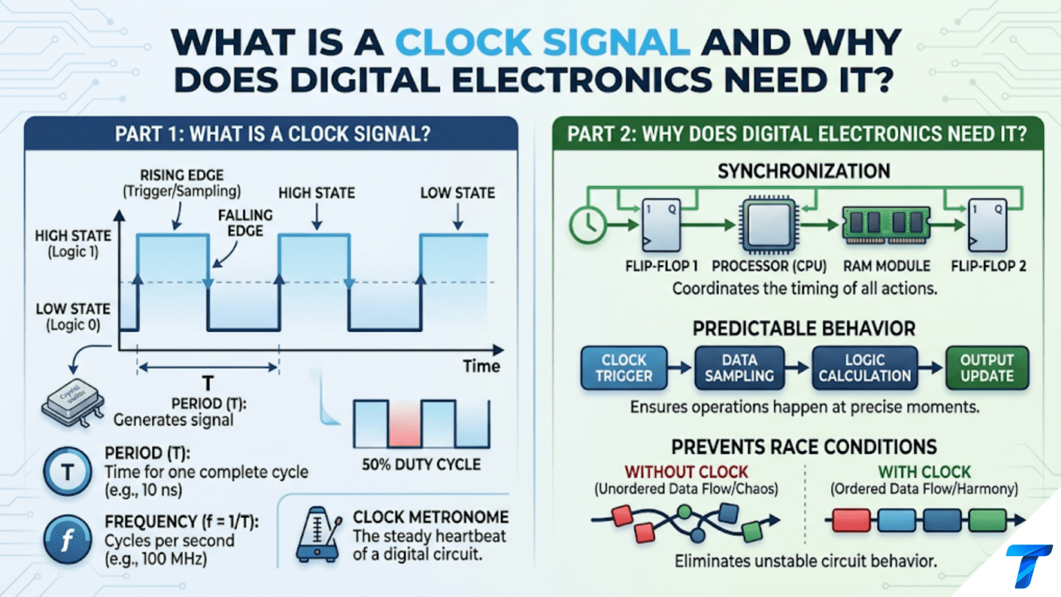
A clock signal is a periodic square wave that alternates between HIGH and LOW at a fixed frequency, providing a shared timing reference for all sequential logic circuits in a digital system. Every flip-flop, register, counter, and state machine captures its input or advances its state on each rising or falling edge of the clock. Without a clock, these circuits have no way to know when to act — data would ripple through flip-flop chains unpredictably and different parts of the system would change state at different, uncoordinated times. The clock is the heartbeat of synchronous digital electronics, ensuring all state changes happen at the same precise instant across the entire system.
Introduction: Coordination at the Heart of Every Digital System
Imagine a factory assembly line. Each station performs one step of the assembly — one worker welds, the next bolts, the next paints. For the line to work, all stations must operate on the same schedule: everyone works for a fixed interval, then everyone advances the product one position. If each worker moved at their own pace, products would pile up at slow stations, and fast workers would grab items before the previous step was complete. The entire system depends on a shared timing signal — a bell, a conveyor belt, a foreman’s whistle — that coordinates every action.
Digital circuits face exactly the same coordination challenge. A complex digital system contains thousands, millions, or billions of logic gates and flip-flops. The output of one flip-flop feeds through combinational logic to become the input of another. That input must be stable and correct before the receiving flip-flop captures it. If one flip-flop acts too early, it captures a transitional garbage value. If it acts too late, it misses the correct value and captures the next one instead. Without coordination, cascades of errors propagate through the system unpredictably.
The clock signal solves this by providing a universal timing reference. Every flip-flop in the system waits for the clock edge before acting. Between edges, all combinational logic settles to its final values. On the edge, every flip-flop simultaneously captures its current input. Then the process repeats. The clock turns the chaos of simultaneously changing logic values into an orderly march of precisely timed state transitions — step, settle, step, settle — at whatever frequency the clock runs.
This article builds a complete understanding of clock signals: why sequential circuits need them, what the clock signal looks like and what its parameters mean, how clock signals are generated from oscillator circuits, the critical relationship between clock frequency and maximum logic propagation delay, clock distribution challenges in real systems, the sources and effects of clock jitter and skew, duty cycle and its importance, and practical circuits for generating and distributing clocks from a single transistor oscillator through to crystal-stabilized and phase-locked loop sources.
Why Sequential Logic Needs a Clock
The Problem Without Timing
Consider two D flip-flops in series with combinational logic between them — the fundamental synchronous design pattern:
Q_A → [combinational logic] → D_B
CLK_A ↑ updates Q_A
CLK_B ↑ updates Q_B from D_BIf both flip-flops are clocked by the same signal, the sequence is:
- Clock edge: FF_A captures its D input, Q_A changes (after t_pCLK-Q delay)
- Q_A propagates through combinational logic, D_B settles to new value (after logic delay)
- Next clock edge: FF_B captures stable D_B → Q_B correctly updated
For this to work, the combinational logic must complete in less than one clock period. Specifically:
t_pCLK-Q + t_logic + t_su < T_clockWhere t_su is FF_B’s setup time. If the logic takes longer than one clock period, FF_B captures a transitional value — wrong result.
The clock period enforces a contract: “all logic will complete within this time window.” The designer’s job is to ensure the slowest combinational path meets this contract. The clock’s job is to provide the synchronizing edges.
What Happens Without a Clock
Without a clock, flip-flops are latches — they respond immediately to input changes. A chain of latches passes data through instantly, with each stage changing as soon as its input changes. This seems faster but creates two serious problems:
Problem 1 — Races: If Q_A’s transition takes a slightly different time than expected (due to temperature, supply voltage, or process variation), D_B may see the new value or the old value — unpredictably. The timing depends on physical variations that cannot be controlled.
Problem 2 — Hazards: As combinational logic transitions from old to new output, intermediate glitch values can pass through — spikes that never represent a valid logical result but may be captured by a downstream latch.
The clock edge creates a sharp, defined boundary: “capture what is there at THIS exact moment, not before, not after.” It converts the continuous-time, analog-influenced behavior of real transistor circuits into discrete, predictable, reliable state transitions.
Synchronous vs. Asynchronous Design
Synchronous design: All flip-flops share one clock (or a family of related clocks). All state changes happen at clock edges. This is the universal approach for any digital system larger than a few gates. Analyzable, testable, scalable.
Asynchronous design: State changes triggered by signal transitions rather than a clock. Potentially faster (no waiting for the next clock edge) but extremely difficult to design correctly. Race conditions and glitches that synchronous design automatically avoids become design hazards that must be individually analyzed and resolved. Used only in specialized low-power or ultra-high-speed applications where the complexity is justified.
For all practical purposes in this series, digital design means synchronous design, and synchronous design requires a clock.
Clock Signal Parameters
Frequency and Period
The clock frequency f is the number of complete HIGH-LOW cycles per second, measured in Hertz (Hz):
f = 1 / TWhere T is the period — the time for one complete cycle.
Common clock frequencies in digital electronics:
| Application | Typical Clock Frequency |
|---|---|
| Simple flip-flop counter (74HC74) | 1Hz–10MHz |
| Arduino Uno (ATmega328P) | 16MHz |
| Arduino Nano 33 IoT | 48MHz |
| STM32F103 (entry ARM) | 72MHz |
| ESP32 | 240MHz |
| Raspberry Pi 4 | 1.5GHz |
| Modern desktop CPU | 3GHz–5GHz |
| DDR5 memory | 4.8GHz–6.4GHz |
Frequency determines throughput — how many operations per second the system can perform. A 16MHz microcontroller executes approximately 16 million simple instructions per second (one per clock cycle for simple operations). A 3GHz processor executes billions.
Duty Cycle
The duty cycle D is the fraction of each period that the clock is HIGH:
D = t_HIGH / T = t_HIGH × fAn ideal clock has a 50% duty cycle — equal time HIGH and LOW. This matters because:
For positive-edge-triggered flip-flops: Only the rising edge (LOW→HIGH transition) matters directly. The duty cycle determines the interval between the rising edge and the next falling edge (= t_HIGH) and between the falling edge and the next rising edge (= t_LOW = T − t_HIGH). Some logic uses both edges.
For double-data-rate (DDR) systems: DDR memory clocks both the rising AND falling edge to capture data, effectively doubling the data rate. For DDR, duty cycle must be very close to 50% — deviation means one edge arrives earlier/later than expected, reducing timing margins.
For power consumption: A 50% duty cycle with equal rise and fall times minimizes certain types of EMI and switching transients compared to asymmetric duty cycles.
For most synchronous logic: 50% duty cycle is standard and preferable, though any duty cycle above about 20% works as long as t_HIGH > t_setup and t_LOW > t_hold for all flip-flops.
Rise Time and Fall Time
Real clock signals are not perfect square waves — the transitions between LOW and HIGH take a finite time:
Rise time (t_r): Time for the signal to transition from 10% to 90% of V_supply on a rising edge.
Fall time (t_f): Time from 90% to 10% on a falling edge.
For 74HC logic at 5V: rise/fall times of a gate output are approximately 5–10ns.
Slow rise/fall times have several consequences:
- Increased jitter sensitivity: A slow edge means noise on the signal causes the crossing of the flip-flop’s threshold at a slightly different time — translating amplitude noise into timing uncertainty (jitter)
- Increased power consumption: During slow transitions, both PMOS and NMOS transistors in CMOS gates are simultaneously partially on — the “crowbar current” flows for longer
- EMI concerns: Slower edges have lower high-frequency harmonic content (good for EMI), while faster edges generate more high-frequency radiation (bad for EMI)
In practice, clock rise/fall times should be much shorter than the flip-flop setup time. For 74HC (t_su = 5ns): rise time < 1–2ns is desirable. This is easily achieved by CMOS logic gate outputs but may not be met by RC oscillator outputs, which must pass through a Schmitt trigger to sharpen the edge.
Jitter
Jitter is the variation in the clock edge’s arrival time from its expected position. An ideal clock edge arrives at exactly t, 2t, 3t, … where t is the period. Real clocks have edges that arrive at t ± δt, where δt is the jitter.
Sources of jitter:
- Thermal noise in oscillator components (resistors, active devices)
- Power supply noise modulating the oscillator frequency
- Phase noise in the VCO of a PLL
- Accumulated clock buffer delays that vary with temperature and voltage
- Cross-talk from adjacent signal lines coupling noise onto the clock
Why jitter matters: Jitter reduces the available timing margin for flip-flops. If a flip-flop has setup time t_su = 5ns and the clock jitter is ±3ns, then the effective setup margin available for combinational logic is reduced by 3ns in the worst case. The clock edge might arrive 3ns early, leaving only T − t_pCLK-Q − t_logic − t_su − jitter for the logic to complete.
For high-speed systems (hundreds of MHz to GHz), clock jitter becomes a primary design constraint. Crystal oscillators produce jitter of picoseconds to nanoseconds; RC oscillators produce much higher jitter (percent-level timing variation). PLL-based clock synthesis can achieve very low jitter by locking to a stable reference.
Jitter specification types:
- Cycle-to-cycle jitter: Variation between consecutive clock periods. Most relevant for setup/hold timing.
- Period jitter: Standard deviation of the clock period measured over many cycles.
- Phase jitter: Long-term variation relative to an ideal reference. Relevant for serial communication bit synchronization.
Clock Skew
While jitter is variation in time, skew is the spatial variation — different flip-flops in a system receiving the clock edge at different times due to different propagation delays along the distribution paths.
If FF_A sees the clock edge 2ns before FF_B, and FF_A’s Q feeds directly to FF_B’s D (with no other logic), FF_B may receive the new Q_A before FF_B’s clock edge arrives — a hold time violation if the propagation delay is shorter than the skew.
In large ICs (ASICs, FPGAs), the clock distribution network (clock tree) is carefully designed to equalize the arrival time of the clock at every flip-flop — minimizing skew to a few picoseconds. In discrete circuit design, clock skew is less critical (fewer flip-flops, shorter distances) but becomes important in multi-chip designs.
How Clock Signals Are Generated
The RC Oscillator
The simplest clock source: an RC network combined with a Schmitt trigger inverter creates an oscillator.
Basic RC oscillator (74HC14 Schmitt trigger):
VCC
 │
[R]
 │
 ├──── 74HC14 input
 │
[C]
 │
GND

74HC14 output ──── feedback back to the RC node (through R)More precisely: 74HC14 input connected to the RC junction. Output feeds back through R to the input. C connects from input to GND.
Operation:
- When output is HIGH: capacitor charges through R toward V_supply. When voltage reaches V_TH+ (Schmitt upper threshold, ≈3.5V at 5V supply), output switches LOW.
- When output is LOW: capacitor discharges through R toward GND. When voltage falls below V_TH− (≈1.5V), output switches HIGH.
- Process repeats → oscillation.
Approximate frequency:
f ≈ 1 / (2.2 × R × C)For R = 10kΩ, C = 10nF: f ≈ 1/(2.2 × 10,000 × 10×10⁻⁹) = 1/(220µs) ≈ 4.5kHz.
Advantages: Extremely simple. Very inexpensive (one Schmitt trigger gate, one resistor, one capacitor). Easily adjustable — change C for decades of frequency range, or use a variable resistor for continuous adjustment.
Disadvantages: Poor frequency stability. The frequency depends on R and C values, which vary with temperature (R changes ~0.4%/°C for carbon film; C changes with temperature depending on type). Supply voltage variation also affects the Schmitt trigger thresholds and therefore the frequency. Typical stability: ±5% to ±20% depending on component quality and temperature range. Jitter is high — percent-level timing variation.
Suitable for: Non-critical timing — LED blink rates, audio tone generation, motor PWM frequency, sequential logic clocks where ±10% frequency error is acceptable.
Improving stability: Use metal-film resistors (±0.1% tolerance, low temperature coefficient) and NPO/C0G ceramic capacitors (±30ppm/°C) rather than standard resistors and X7R ceramics. This improves stability to ±1–2% but still inferior to crystal oscillators.
The Crystal Oscillator
A quartz crystal is a piezoelectric resonator: applying a voltage causes it to physically vibrate, and its vibration generates a voltage. The mechanical resonance frequency is determined by the crystal’s physical dimensions, cut angle, and mass — properties that are controlled with extreme precision during manufacturing and change very little with temperature.
Crystal frequency stability: ±20ppm (parts per million) for standard crystals. At 16MHz, ±20ppm = ±320Hz — the frequency stays between 15,999,680Hz and 16,000,320Hz across the rated temperature range. Compare to an RC oscillator at ±5%: ±800,000Hz variation at 16MHz. The crystal is 2,500× more stable.
Typical crystal oscillator circuit for microcontrollers:
Most microcontrollers include an on-chip crystal oscillator circuit — just connect a crystal and two small load capacitors:
MCU XTAL1 pin ──┬── Crystal ──┬── MCU XTAL2 pin
                │             │
               [C1]          [C2]
                │             │
GND GNDLoad capacitor values (C1, C2) are specified by both the microcontroller and crystal datasheets — typically 12–22pF for standard AT-cut crystals. Using the wrong value shifts the oscillation frequency slightly.
Arduino Uno / ATmega328P: 16MHz crystal with 22pF load capacitors. The internal oscillator circuit drives the crystal and produces the system clock.
Crystal oscillator modules: Self-contained units (DIP-4 or SMD packages) containing the crystal, oscillator circuit, and output buffer. Just apply power and a stable, buffered clock output is available. Frequencies from 1MHz to 200MHz. Much easier to use than discrete crystal circuits. Cost: $0.50–$2.00.
Temperature-compensated crystal oscillators (TCXO): Add a temperature sensor and voltage-controlled capacitor to continuously correct for temperature-dependent frequency drift. Achieve ±1–2ppm stability. Used in GPS receivers, precision measurement instruments, cellular base stations.
Oven-controlled crystal oscillators (OCXO): Place the crystal in a temperature-controlled oven held at a constant temperature. Achieve ±0.01–0.001ppm stability (10–1000× better than TCXO). Used in scientific instruments, atomic clock references, frequency standards.
The 555 Timer as a Clock
The 555 timer in astable mode produces a square wave suitable as a clock for low-speed applications. Frequency is set by two resistors and a capacitor:
f = 1.44 / ((R1 + 2×R2) × C)Duty cycle: D = (R1 + R2) / (R1 + 2×R2) — not easily set to 50% with a standard 555 configuration. For 50% duty cycle, use R1 ≈ 0 (short) and R2 large, or use the CMOS 555 variant with a modification.
Stability: Better than a bare RC oscillator because the 555 uses comparator thresholds referenced to 2/3 and 1/3 of V_supply, which track supply voltage changes. Still dependent on R and C values (±5–10% typically). Not suitable for applications requiring precise frequency.
Useful for: Visual counter clocks (1Hz), audio tone generators, LED flashers, teaching demonstrations of sequential logic circuits.
Accurate 1Hz using 555: R1 = 1kΩ, R2 = 360kΩ, C = 2.2µF → f = 1.44/(722,000 × 2.2×10⁻⁶) = 1.44/1.588 ≈ 0.907Hz. Adjust R2 to approximately 390kΩ for f ≈ 1Hz.
The Phase-Locked Loop (PLL)
A PLL is a feedback control system that generates an output clock phase-locked to (synchronized with) an input reference clock. By using a frequency divider in the feedback path, the PLL can multiply the reference frequency:
f_out = N × f_referenceWhere N is the integer (or fractional) division ratio.
PLL components:
- Phase-frequency detector (PFD): Compares the phase and frequency of the reference clock to the feedback clock, generating an error signal proportional to the phase difference
- Charge pump + loop filter: Converts the PFD error signal to a smooth voltage
- Voltage-controlled oscillator (VCO): Generates the output clock at a frequency proportional to its input voltage
- Frequency divider (÷N): Divides the VCO output frequency by N and feeds it back to the PFD
In lock: The feedback frequency (f_out/N) equals the reference frequency. f_out = N × f_ref. The VCO runs stably at the desired output frequency, correcting for any drift.
Applications in microcontrollers: Nearly every modern microcontroller uses an internal PLL to multiply a low-frequency reference (often 4–16MHz crystal) up to a higher system clock (72MHz for STM32F103, 240MHz for ESP32). This allows using a common, standard crystal frequency while operating the core at whatever frequency is needed.
External PLL ICs: Si5351A (Silicon Labs) — generates up to three independent clock outputs from 8kHz to 160MHz, all phase-locked to a single reference crystal. Configurable over I²C. Used in software-defined radio, signal generators, and test equipment to generate arbitrary frequencies. About $1 each.
The Clock Constraint: Speed vs. Logic Depth
The Fundamental Timing Equation
Every synchronous digital circuit must satisfy:
T_clock > t_pCLK-Q + t_logic + t_suRearranging for maximum frequency:
f_max = 1 / (t_pCLK-Q + t_logic_max + t_su)Where t_logic_max is the propagation delay through the LONGEST combinational path between any two flip-flops in the system (the critical path).
For 74HC logic at 5V:
- t_pCLK-Q (74HC74): 14ns
- t_su (74HC74): 5ns
- t_pd per gate (74HC): ~7ns
For a circuit with 3 levels of combinational logic (3 gates in the critical path):
f_max = 1 / (14 + 3×7 + 5) = 1 / 40ns = 25MHzFor 5 levels:
f_max = 1 / (14 + 5×7 + 5) = 1 / 54ns = 18.5MHzThis is why minimizing gate depth in the critical path is a central concern of digital design for speed.
Hold Time Constraint
The clock must also satisfy a minimum timing constraint to prevent hold time violations:
t_pCLK-Q_min + t_logic_min > t_holdThe logic path must take at least t_hold time. If the path between two flip-flops is too short (e.g., direct Q→D connection), the new Q value arrives at D before t_hold has elapsed after the common clock edge — the flip-flop captures the wrong (new) value instead of the (old) correct one.
Hold time violations:
- Cannot be fixed by slowing the clock — they exist regardless of clock frequency
- Require adding delay in the short path (insert buffer gates, increase wire length)
- Are more common in very fast technologies (where t_pCLK-Q < t_hold) than in 74HC-speed designs
For 74HC74: t_hold = 5ns, t_pCLK-Q_min ≈ 5ns. Direct Q→D connection: 5ns ≥ 5ns — borderline. Any PCB trace delay adds margin. Usually fine in practice with 74HC, but must be checked for faster logic families.
Pipeline Stages Increase Throughput
For a computation requiring 10 gate levels (10 × 7ns = 70ns logic delay), the maximum clock is:
f_max = 1 / (14 + 70 + 5) = 1 / 89ns = 11.2MHzBy inserting a pipeline register in the middle (after 5 gate levels), the critical path becomes 5 gates:
f_max_pipelined = 1 / (14 + 35 + 5) = 1 / 54ns = 18.5MHzThe system runs 65% faster. The result still takes 2 clock cycles to emerge (latency doubles), but the throughput (results per second) increases. This pipeline tradeoff — increased latency for increased throughput — is exploited throughout digital design from simple adders to billion-transistor processors.
Clock Distribution in Real Systems
The Clock Tree
In a complex digital system (FPGA, ASIC, or microcontroller), the clock signal must reach thousands or millions of flip-flops. The clock distribution network — the clock tree — must deliver the clock to every flip-flop with:
- Minimum skew (all edges arrive at the same time)
- Low jitter (edges are sharp and well-timed)
- Sufficient drive strength (the clock net has enormous capacitive load from all those flip-flop clock inputs)
A clock tree uses a balanced binary tree of clock buffers, each driving exactly two sub-trees of equal capacitance. Because each path from root to leaf has the same number of buffers and the same total capacitance, all edges arrive at the same time.
In modern FPGAs, dedicated global clock networks with matched routing guarantee picosecond-level skew across the entire device. Regular routing would introduce nanoseconds of skew across a large die.
Discrete Circuit Clock Distribution
In circuits using discrete logic ICs (74HC series), clock distribution is simpler but still requires attention:
Fanout: The clock signal may need to drive many IC inputs simultaneously. Each 74HC input presents a few picofarads of input capacitance. For 20 ICs × 5pF each = 100pF total. Driving 100pF from a 74HC gate output through PCB traces: OK for frequencies below ~50MHz.
For higher frequencies or larger fanout, use a dedicated clock buffer/driver with higher current output and multiple outputs: SN74AHCT1G125 (single buffer), SN74HC4050 (hex buffer), or dedicated clock distribution ICs (DS1003, CDCLVC1310).
Trace routing: Clock traces on PCBs should be kept short and equal length to all destinations. Long traces add capacitive load (slowing edges), inductance (causing ringing on fast edges), and delay (adding skew between near and far destinations).
Termination: At frequencies above ~100MHz on PCBs, transmission line effects become important. Clock traces may need series termination (25–50Ω resistor at the driver) or parallel termination (50Ω to GND at the receiver) to prevent reflections that cause ringing.
Practical Clock Circuits
Circuit 1: Adjustable RC Clock for Sequential Logic
Application: Provide an adjustable 1Hz–100kHz clock for a counter or state machine demonstration circuit.
Components:
- 74HC14 (hex Schmitt trigger inverter)
- 100kΩ variable resistor (potentiometer)
- 10kΩ fixed resistor (minimum R for stability)
- 10nF film capacitor (C0G for best stability)
- 100Ω output resistor (reduces overshoot on clock output)
Circuit:
VCC ─[100kΩ pot + 10kΩ fixed]─┬─── 74HC14 pin 1 (input)
                              │
                          [10nF C0G]
                              │
                             GND

74HC14 pin 2 (output) ─┐─── output to clock consumer circuits
                       │
                 [100Ω series]─── buffered clock output

Also: 74HC14 pin 2 → 74HC14 pin 3 → pin 4 → output [buffer chain for drive strength]Frequency range calculation:
At maximum R (100kΩ + 10kΩ = 110kΩ): f = 1/(2.2 × 110,000 × 10×10⁻⁹) = 1/2.42ms ≈ 413Hz At minimum R (10kΩ only): f = 1/(2.2 × 10,000 × 10×10⁻⁹) = 1/220µs ≈ 4.5kHz
For 1Hz–100Hz range: change C to 10µF. For 10kHz–100kHz range: change C to 1nF.
Stability improvement: Power the 74HC14 and oscillator circuit from a separate, well-regulated supply. Use an LM7805 or LP2950 dedicated to the oscillator. Noise on V_supply modulates the Schmitt trigger thresholds and causes frequency jitter. A stable supply dramatically improves oscillator stability.
Circuit 2: Crystal Clock for Microcontroller (Arduino/ATmega328P)
Application: Provide the standard 16MHz system clock for an ATmega328P running custom firmware (bare-metal, not using Arduino bootloader’s internal RC oscillator).
Circuit:
XTAL1 (MCU pin 7) ──┬── Y1 (16MHz crystal) ──┬── XTAL2 (MCU pin 8)
                    │                        │
                  [22pF]                  [22pF]
                    │                        │
GND GNDComponent selection:
- Crystal: HC-49/S or HC-49/US package, 16.000MHz, ±20ppm, parallel resonance, 18pF load capacitance
- Capacitors: 22pF ±5% NPO/C0G ceramic (not X5R or X7R which change capacitance with voltage)
Fuse bits: The ATmega328P must have its fuse bits set to use the external crystal oscillator (CKSEL = 1111 for external full-swing crystal oscillator). Incorrect fuse bits cause the MCU to ignore the external crystal and use its internal 8MHz RC oscillator instead.
Why 22pF load capacitors: The crystal has a specified load capacitance (typically 18pF). The two external capacitors appear in series from the crystal’s perspective, with parasitic PCB capacitance (~2–5pF per node):
C_load = (C1 × C2)/(C1 + C2) + C_stray
= (22 × 22)/(22 + 22) + 3 ≈ 11 + 3 = 14pFThis is slightly below the crystal’s 18pF load specification — use 27pF capacitors for a closer match (13.5 + 3 = 16.5pF). The exact value shifts the crystal frequency by a few ppm — negligible for most applications but important for precision timing.
Circuit 3: Crystal Oscillator Module for Multiple Consumers
Application: Generate a 10MHz reference clock for a digital circuit board containing multiple 74HC ICs (counters, flip-flops, shift registers). Use a pre-made crystal oscillator module for simplicity and reliability.
Oscillator module selection: DIP-4 half-size crystal oscillator module, 10.000MHz, ±50ppm, HCMOS output, 5V supply. Cost: ~$1.50.
Module pinout (standard half-DIP-4):
- Pin 1: Output Enable (tie HIGH for always-on)
- Pin 8: GND
- Pin 14: Output
- Pin 16: VCC
Output buffering for multiple loads:
The oscillator module output drives a 74HC04 buffer (or 74HC00 NAND with inputs tied together):
OSC module output → 74HC04 pin 1 (input)
74HC04 pin 2 (output 1) → CLK input, 74HC163 counter #1
74HC04 pin 4 (output 2) → CLK input, 74HC163 counter #2
74HC04 pin 6 (output 3) → CLK input, 74HC74 flip-flops
[two more outputs for additional loads]Using one gate per destination ensures each consumer sees a buffered, low-impedance clock source rather than competing for current from a single driver.
Decoupling: 100nF ceramic capacitor directly at the oscillator module’s VCC and GND pins. 100nF at each 74HC04 VCC pin. Critical — switching current pulses at 10MHz (100ns period) require local charge reservoirs.
Circuit 4: 1Hz Clock from 32.768kHz Watch Crystal
Application: Generate an accurate 1Hz timebase for a clock circuit, using a 32.768kHz crystal (2^15 Hz) divided by 2^15 = 32,768. Extremely common in real-time clock (RTC) circuits.
Why 32.768kHz: This specific frequency equals 2^15 Hz. Dividing by 2^15 (fifteen binary divide-by-2 stages, i.e., fifteen flip-flops in a chain) gives exactly 1Hz. The number was chosen specifically for this property.
32.768kHz crystal oscillator circuit:
A standard inverter oscillator using a CMOS inverter (74HC04 or CD4069):
XTAL (32.768kHz) connects between inverter input and output.
R_feedback (10MΩ) biases the inverter in its linear region (across inverter: output to input).
C1 (12pF) from input to GND.
C2 (12pF) from output to GND.
Output through 1kΩ series resistor to prevent loading the crystal.The high-value feedback resistor (10MΩ) is critical — it biases the CMOS inverter into its linear region where gain is high, creating the amplifier needed for oscillation. Without it, the inverter’s digital switching action would interfere with the crystal resonance.
Division chain:
A 15-stage binary ripple counter divides 32,768Hz by 32,768:
Using two CD4020 (14-stage binary counter) ICs or the CD4060 (14-stage counter with built-in oscillator circuit):
CD4060: Contains the crystal oscillator circuit AND 14 binary divider stages internally. Connect the 32.768kHz crystal with feedback resistor and two load capacitors to the XTAL pins. Q13 output (after 2^14 = 16,384 division): 32,768/16,384 = 2Hz. Adding one external flip-flop (74HC74) for the 15th division: 2Hz/2 = 1Hz.
Complete 1Hz clock:
32.768kHz crystal + CD4060 + one 74HC74 flip-flop = accurate 1Hz
Accuracy: ±20ppm = ±0.63 seconds per yearThis is the exact architecture used in virtually every digital wall clock, wristwatch (quartz analog and digital), real-time clock IC (DS1307, PCF8523), and microcontroller RTC peripheral.
Circuit 5: Variable-Frequency Clock Using Si5351A PLL
Application: Generate programmable clock frequencies from 8kHz to 160MHz for a software-defined radio, signal generator, or test instrument. Control via I²C from a microcontroller.
Si5351A features:
- Three independent clock outputs (CLK0, CLK1, CLK2)
- Frequency range: 8kHz to 160MHz per output
- Phase-locked to a 25MHz or 27MHz reference crystal
- Resolution: sub-Hz at low frequencies, ~0.01Hz at high frequencies
- Phase adjustment: independent phase offset per output, in 1/4-cycle steps
- I²C interface: address 0x60 (default)
- Supply: 3.3V, 7mA quiescent
- Package: QFN-20 or evaluation module breakouts available (~$1 bare IC)
Arduino code for Si5351A using Etherkit library:
#include <si5351.h>
#include <Wire.h>

Si5351 si5351;

void setup() {
  Wire.begin();
  si5351.init(SI5351_CRYSTAL_LOAD_8PF, 0, 0);
  // 0 = use default 25MHz crystal; last arg = frequency correction in ppb

  // Set CLK0 to 10MHz
  si5351.set_freq(1000000000ULL, SI5351_CLK0);
  // Frequency in hundredths of Hz: 10MHz = 1,000,000,000 / 100 = 10,000,000 Hz
  // Actually: 10MHz = 10,000,000 Hz = 1,000,000,000 in units of 0.01 Hz

  // Set CLK1 to 14.318MHz (common video clock)
  si5351.set_freq(1431800000ULL, SI5351_CLK1);

  // Set CLK2 to 27MHz (common reference)
  si5351.set_freq(2700000000ULL, SI5351_CLK2);

  // Enable outputs
  si5351.output_enable(SI5351_CLK0, 1);
  si5351.output_enable(SI5351_CLK1, 1);
  si5351.output_enable(SI5351_CLK2, 1);
}

void loop() {
  // Sweep CLK0 from 1MHz to 100MHz in 1MHz steps
  for (uint64_t freq = 100000000ULL; freq <= 10000000000ULL; freq += 100000000ULL) {
    si5351.set_freq(freq, SI5351_CLK0);
    delay(100);
  }
}Output jitter: Si5351A achieves approximately 100–300ps RMS jitter at output frequencies above 1MHz — excellent for most applications though not suitable for the most demanding high-speed serial links.
Common Clock Circuit Mistakes
Mistake 1: No decoupling on the clock oscillator supply
The oscillator’s power supply must be clean and stable — every millivolt of supply noise translates to picoseconds to nanoseconds of jitter. Place 100nF ceramic directly at the oscillator module’s VCC pin. For crystal oscillator circuits, place 100nF at the IC’s VCC as well. Consider a small series resistor (10Ω) + decoupling capacitor (100nF) as a local filter from the main supply.
Mistake 2: Driving many gate inputs directly from a single clock source
Excessive capacitive load on the clock driver slows the clock edges, increasing jitter and potentially violating setup times for fast logic. Buffer the clock with a dedicated clock buffer IC or fan it out through multiple inverters (one inverter per group of 5–10 loads). Using clock distribution ICs ensures matched, buffered outputs to all consumers.
Mistake 3: Running clock traces near noisy signals
Clock traces are extremely sensitive to crosstalk because they run at full supply swing on every single cycle. Route clock traces away from high-current switching lines (motor PWM, LED drive), between ground planes if possible, and with guard traces on either side connected to GND for critical high-speed designs.
Mistake 4: Using an RC oscillator for timing-critical applications
An RC oscillator varying ±10% may cause UART baud rate errors (UART tolerates only ±2–3% baud rate error), incorrect timer intervals in real-time systems, or frequency counting errors. Use a crystal oscillator for any application where frequency accuracy matters.
Mistake 5: Crystal circuit with wrong load capacitors
Using wrong capacitor values for the crystal oscillator causes the crystal to run off-frequency, oscillate weakly (or not at all in severe cases), or oscillate at an overtone frequency (3× or 5× the fundamental). Always follow both the microcontroller datasheet AND the crystal datasheet for load capacitor recommendations.
Mistake 6: Forgetting hold time violations in short paths
When the clock is fast enough that t_pCLK-Q < t_hold for a fast flip-flop, a direct Q→D connection (as in a counter or shift register) may violate hold time. This is rare with 74HC logic at room temperature but can occur with faster logic families (74ACT, ECL). Verify hold time margins for all short data paths.
Summary
The clock signal is the universal timing coordinator of synchronous digital electronics — a periodic square wave whose edges simultaneously trigger state changes in every flip-flop, register, and counter in the system. Without a clock, sequential logic races and glitches unpredictably. With a clock, all state transitions happen at precise, controllable instants, making complex digital systems analyzable and reliable.
Four key clock parameters define its behavior: frequency (operations per second, limited by the critical combinational path via t_pCLK-Q + t_logic + t_su < T_clock), duty cycle (typically 50% for most logic; critical for DDR systems), jitter (timing variation that erodes setup/hold margins), and skew (spatial variation in clock arrival time across the system).
Clock sources range in cost, complexity, and accuracy: RC oscillators with 74HC14 Schmitt triggers are simple and cheap but ±5–20% stable; crystal oscillators (±20ppm, ≈±0.002%) are the standard for any frequency-accurate application; PLL-based oscillators (Si5351A, internal MCU PLLs) multiply a reference to generate high frequencies with low jitter; TCXO and OCXO types achieve ±1ppm and ±0.001ppm for precision instruments.
The practical circuits — adjustable RC clock, 16MHz crystal for ATmega328P, 10MHz oscillator module with buffered distribution, 1Hz from 32.768kHz (CD4060 + flip-flop), and programmable Si5351A PLL — cover the full range from simple learning circuits to professional signal generation, providing the timing foundation that every circuit in this series depends on.