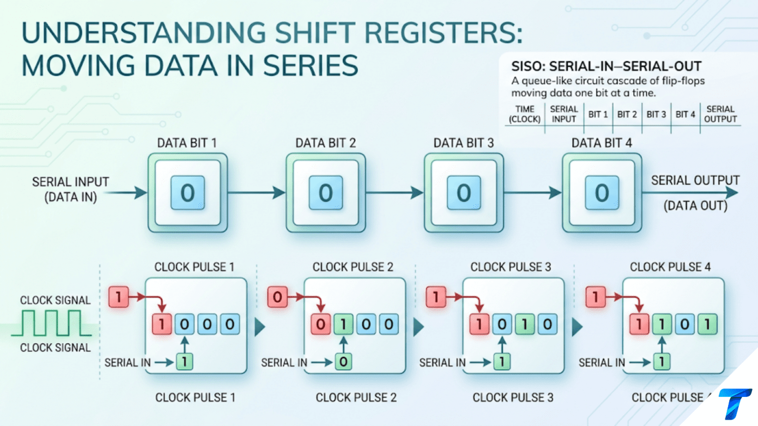
A shift register is a chain of D flip-flops connected so that each flip-flop’s Q output feeds the next flip-flop’s D input, all sharing a common clock. On each clock pulse, every bit shifts one position along the chain — data enters at one end and moves toward the other. Shift registers convert between serial and parallel data formats: feeding data in one bit at a time (serial-in) produces all bits simultaneously at the outputs (parallel-out), and loading all bits simultaneously (parallel-in) allows them to be read out one at a time (serial-out). This makes shift registers essential for expanding microcontroller I/O, driving LED arrays, interfacing SPI devices, and transmitting data over minimal wire connections.
Introduction: When You Need More Outputs Than Pins
Every microcontroller has a limited number of GPIO pins. An Arduino Uno has 20 usable I/O pins. An ESP32 has around 34. Even a powerful ARM processor on a development board may expose only 50–80 pins to the user. Yet real-world applications frequently demand more: driving 32 individual LEDs, scanning a 64-key keyboard matrix, controlling a large seven-segment display, or managing dozens of relays and solenoids.
The traditional solution — using a larger microcontroller with more pins — quickly becomes uneconomical and physically impractical. The elegant solution is the shift register: a circuit that multiplies the effective number of outputs from just two or three pins.
With a 74HC595 serial-in parallel-out shift register, three microcontroller pins (data, clock, latch) control eight independent output bits. Chain two 74HC595s and those same three pins control sixteen outputs. Chain four and you have thirty-two outputs — all from three wires. The data rate is slower than direct GPIO (a few microseconds per bit rather than nanoseconds), but for most output applications — LEDs, relays, display digits — this is more than fast enough.
The reverse operation is equally valuable. A 74HC165 parallel-in serial-out shift register reads eight independent inputs and delivers them serially over two wires to a microcontroller. An eight-button keypad, eight limit switches, or eight DIP switches become readable with just two pins instead of eight.
Shift registers are also fundamental to serial communication protocols. SPI (Serial Peripheral Interface) is essentially a coordinated pair of shift registers — one in the master, one in the slave — exchanging data simultaneously. UART serial transmission sends data through a shift register that converts between the processor’s parallel internal data bus and the single-wire serial output. Understanding shift registers means understanding the mechanism behind all serial communication.
This article builds a complete, practical understanding of shift registers: the flip-flop chain that creates the shift behavior, the four configurations (SIPO, PISO, SISO, PIPO), timing diagrams that show exactly what happens on each clock edge, the 74HC595 and 74HC165 ICs in full detail with every pin explained, chaining multiple shift registers, and five complete design examples spanning LED matrix driving, button scanning, 7-segment multiplexing, and SPI peripheral interfacing.
The Shift Register Mechanism: Flip-Flops in a Chain
The Basic Chain
Take four D flip-flops. Connect Q of each to D of the next, sharing a common clock:
SERIAL_IN → [FF0] → [FF1] → [FF2] → [FF3] → SERIAL_OUT
Q0 → D1 Q1 → D2 Q2 → D3On each rising clock edge, every flip-flop captures what is currently on its D input:
- FF0 captures SERIAL_IN
- FF1 captures Q0 (what FF0 held before this clock edge)
- FF2 captures Q1 (what FF1 held before this clock edge)
- FF3 captures Q2 (what FF2 held before this clock edge)
The result: each flip-flop’s previous value moves one position to the right. Data shifts along the chain, one position per clock cycle.
A Shift Operation Traced in Detail
Load the bit pattern 1011 serially, MSB first (1, 0, 1, 1 — four clock pulses):
Before any clocks (all zeros):
| FF0 (Q0) | FF1 (Q1) | FF2 (Q2) | FF3 (Q3) |
|---|---|---|---|
| 0 | 0 | 0 | 0 |
Apply SERIAL_IN = 1, Clock ↑ (pulse 1):
| Q0 | Q1 | Q2 | Q3 |
|---|---|---|---|
| 1 | 0 | 0 | 0 |
FF0 captures SERIAL_IN=1. Others capture previous neighbor (all 0).
Apply SERIAL_IN = 0, Clock ↑ (pulse 2):
| Q0 | Q1 | Q2 | Q3 |
|---|---|---|---|
| 0 | 1 | 0 | 0 |
FF0 captures SERIAL_IN=0. FF1 captures previous Q0=1. Others shift right.
Apply SERIAL_IN = 1, Clock ↑ (pulse 3):
| Q0 | Q1 | Q2 | Q3 |
|---|---|---|---|
| 1 | 0 | 1 | 0 |
Apply SERIAL_IN = 1, Clock ↑ (pulse 4):
| Q0 | Q1 | Q2 | Q3 |
|---|---|---|---|
| 1 | 1 | 0 | 1 |
After 4 clock pulses, the register contains: Q3 Q2 Q1 Q0 = 1 0 1 1.
Reading Q3 (MSB) to Q0 (LSB): 1011 — the exact 4-bit pattern loaded serially. The serial input has been converted to parallel output. This is serial-to-parallel conversion: the fundamental operation of a SIPO (Serial-In Parallel-Out) shift register.
The Critical Timing Rule
All flip-flops update simultaneously on the same clock edge. This is what makes the shift work correctly: FF1 captures FF0’s OLD value (from before the clock edge), not FF0’s new value. If the flip-flops were transparent latches instead of edge-triggered, the new value would race through the entire chain in one clock cycle — no controlled shifting.
This simultaneous capture (hold time allowing FF0’s old Q to remain stable long enough for FF1 to capture it) is guaranteed by the flip-flop’s setup/hold time relationship: Q0 changes approximately 14ns after the clock edge (t_pCLK-Q), while FF1’s hold time requirement is only 5ns. By the time Q0 changes (14ns after clock), FF1 has already captured the stable old value of Q0 (held since 5ns after clock). The shift works correctly without any additional timing hardware.
The Four Shift Register Configurations
SIPO — Serial In, Parallel Out
Data enters one bit at a time; all bits appear simultaneously at the outputs.
- Input: 1 serial data wire + 1 clock wire = 2 wires
- Output: N parallel output bits
- Use cases: expanding microcontroller outputs, driving LED arrays, generating parallel control signals
This is the mode described in the example above. After N clock pulses, the N input bits appear simultaneously on Q0 through Q_{N-1}. This is how 74HC595 works.
Timing: N clock cycles required to load N bits. After those N cycles, all outputs are simultaneously valid.
PISO — Parallel In, Serial Out
All bits loaded simultaneously; bits emerge one at a time.
- Input: N parallel data inputs + 1 load signal + 1 clock wire
- Output: 1 serial data wire
- Use cases: reading multiple switch states into a microcontroller, sending parallel bus data over a serial link
Load all bits at once (one clock edge with the LOAD signal asserted). Then shift out: each clock pulse moves the chain one position, presenting each bit in turn at the serial output. After N clock pulses all N bits have been read out.
This is how 74HC165 works.
SISO — Serial In, Serial Out
Data enters serially at one end and exits serially at the other end after N clock delays.
- Input: 1 serial wire + 1 clock
- Output: 1 serial wire (delayed N clock cycles from input)
- Use cases: time delay lines, pipeline registers, data synchronization buffers
The SISO shift register is a digital delay line. Data appears at the output exactly N clock cycles after entering the input. Useful for synchronizing signals that must be aligned in time, creating tap-delay lines for FIR filters, or pipeline staging in signal processing.
PIPO — Parallel In, Parallel Out
All bits loaded simultaneously; all bits available simultaneously. Output updates on each clock.
- Input: N parallel inputs + 1 clock
- Output: N parallel outputs
- Use cases: pipeline register between logic stages, synchronous data bus register, delay-by-one-clock-cycle
Technically any D flip-flop register (74HC273, 74HC374) implements PIPO. All bits are loaded from the parallel inputs on each clock edge and appear at parallel outputs one propagation delay later.
The 74HC595: Serial-In Parallel-Out with Storage Register
The 74HC595 is one of the most widely used ICs in hobbyist and professional electronics, appearing in everything from LED matrix drivers to industrial control panels. Its combination of serial input, parallel output, and output latch makes it the standard solution for I/O expansion.
Internal Architecture
The 74HC595 contains two registers in series:
Shift register (8-bit): A standard 8-bit SIPO shift register. Data clocked in via the SER (serial data) pin on rising edges of SRCLK (shift register clock). The shift register’s contents are invisible to the outside — they do not affect the output pins.
Storage (output) register (8-bit): A separate 8-bit register holding the current output state. Contents transfer from the shift register to the storage register on the rising edge of RCLK (register clock, also called latch clock). The QA–QH output pins reflect whatever is in the storage register.
This two-stage architecture is what makes the 74HC595 so useful. While new data is being shifted in (one bit at a time, shifting all 8 positions), the current output register contents remain stable — the outputs do not flicker or show intermediate states during loading. Only when RCLK pulses does the new data appear at the outputs — all eight bits updating simultaneously.
74HC595 Pin Assignments (16-pin DIP/SOIC)
| Pin | Name | Function |
|---|---|---|
| 1 | QB | Parallel output bit 1 |
| 2 | QC | Parallel output bit 2 |
| 3 | QD | Parallel output bit 3 |
| 4 | QE | Parallel output bit 4 |
| 5 | QF | Parallel output bit 5 |
| 6 | QG | Parallel output bit 6 |
| 7 | QH | Parallel output bit 7 |
| 8 | GND | Ground |
| 9 | QH’ | Serial output (for daisy-chaining) |
| 10 | SRCLR̅ | Shift register clear (active-LOW; tie HIGH for normal use) |
| 11 | SRCLK | Shift register clock (data shifts in on rising edge) |
| 12 | RCLK | Storage register clock / latch (outputs update on rising edge) |
| 13 | OE̅ | Output enable (active-LOW; tie LOW for always-enabled outputs) |
| 14 | SER | Serial data input |
| 15 | QA | Parallel output bit 0 (first bit shifted in) |
| 16 | VCC | Supply (2V–6V) |
Critical pin notes:
- SRCLR̅ (pin 10): Always tie to VCC for normal operation. If pulled LOW, clears the shift register (not the output register). Useful for initialization but causes confusion if left floating.
- OE̅ (pin 13): Always tie to GND for always-enabled outputs. If HIGH, all QA–QH go high-impedance (tri-state). Useful for bus sharing; a potential source of bugs if floating.
- QH’ (pin 9): This is the serial output — the last bit shifted through the 8-stage register. Connect this to the SER input of the next 74HC595 when daisy-chaining for more than 8 outputs.
Timing Diagram
SER:   ─ D7 ─ D6 ─ D5 ─ D4 ─ D3 ─ D2 ─ D1 ─ D0 ─
SRCLK: _┐_┐_┐_┐_┐_┐_┐_┐_
        ↑  ↑  ↑  ↑  ↑  ↑  ↑  ↑  (8 rising edges shift in D7..D0)
RCLK:  ________________________________┐___
                                        ↑ (one rising edge latches outputs)
QA-QH: ─────────────────────────────── D7..D0 valid ─SER data must be stable before each SRCLK rising edge (setup time ~5ns for 74HC). RCLK pulse latches all 8 bits simultaneously to the output pins. The outputs remain stable until the next RCLK pulse.
Sending Data to 74HC595 from a Microcontroller
Method 1: Bit-banging (any GPIO pins, software control):
const int SER_PIN   = 11;  // Data pin
const int SRCLK_PIN = 12;  // Shift clock
const int RCLK_PIN  = 10;  // Latch clock

void shiftOut595(uint8_t data) {
  // Shift out 8 bits, MSB first
  for (int i = 7; i >= 0; i--) {
    // Set data bit
    digitalWrite(SER_PIN, (data >> i) & 1);
    // Clock it in
    digitalWrite(SRCLK_PIN, HIGH);
    delayMicroseconds(1);  // Ensure setup/hold times met
    digitalWrite(SRCLK_PIN, LOW);
    delayMicroseconds(1);
  }
  // Latch to outputs
  digitalWrite(RCLK_PIN, HIGH);
  delayMicroseconds(1);
  digitalWrite(RCLK_PIN, LOW);
}

void setup() {
  pinMode(SER_PIN, OUTPUT);
  pinMode(SRCLK_PIN, OUTPUT);
  pinMode(RCLK_PIN, OUTPUT);
  shiftOut595(0b10110001);  // Set outputs: QH=1,QG=0,QF=1,QE=1,QD=0,QC=0,QB=0,QA=1
}Method 2: Hardware SPI (much faster):
The Arduino’s SPI peripheral can drive a 74HC595 at up to 8MHz, shifting 8 bits in about 1µs instead of 16µs for bit-bang at 500kHz:
#include <SPI.h>

const int RCLK_PIN = 10;  // Latch — use any GPIO pin

void setup() {
  pinMode(RCLK_PIN, OUTPUT);
  SPI.begin();
  SPI.beginTransaction(SPISettings(8000000, MSBFIRST, SPI_MODE0));
}

void write595(uint8_t data) {
  digitalWrite(RCLK_PIN, LOW);
  SPI.transfer(data);
  digitalWrite(RCLK_PIN, HIGH);
  digitalWrite(RCLK_PIN, LOW);  // Pulse high then return low
}Arduino’s SPI uses: MOSI → SER, SCK → SRCLK, any GPIO → RCLK. MISO is unused (unless reading QH’ for verification).
Daisy-Chaining 74HC595s
To control 16 outputs from 3 pins, chain two 74HC595s:
MCU → SER → [595 #1] → QH'(pin9) → SER → [595 #2]
MCU → SRCLK → both 595s (shared clock)
MCU → RCLK → both 595s (shared latch)All 16 shift register positions form one long 16-bit chain. Send 16 bits serially (MSB of the second chip first, then MSB of the first chip, down to LSB of the first chip). One RCLK pulse latches all 16 bits simultaneously.
Code for two chained 74HC595s:
void write595_16(uint16_t data) {
  digitalWrite(RCLK_PIN, LOW);
  // Send high byte first (it shifts through to 595 #2 as 595 #1 fills)
  SPI.transfer((data >> 8) & 0xFF);  // High byte → ends up in 595 #2
  SPI.transfer(data & 0xFF);          // Low byte → ends up in 595 #1
  digitalWrite(RCLK_PIN, HIGH);
  digitalWrite(RCLK_PIN, LOW);
}Each additional 74HC595 adds 8 more outputs with no additional MCU pins. Four ICs = 32 outputs from 3 pins.
Maximum chain length: Limited by timing — the serial data must propagate through all QH’ connections to reach the last chip before the final SRCLK edge. At 8MHz SPI, the bit period is 125ns. Each QH’ output has a propagation delay of ~14ns. A chain of 10 ICs adds 140ns of cumulative delay — manageable at 8MHz. At extremely long chains (20+ ICs) or high frequencies, reduce the SPI clock to ensure reliable shifting.
The 74HC165: Parallel-In Serial-Out
The 74HC165 is the complement to the 74HC595 — it reads 8 parallel inputs and shifts them out serially, allowing a microcontroller to read 8 inputs using only 2 pins (plus 1 for load strobe).
74HC165 Pin Assignments (16-pin DIP/SOIC)
| Pin | Name | Function |
|---|---|---|
| 1 | PL̅ | Parallel Load (active-LOW: loads A-H inputs when LOW) |
| 2 | CP | Clock pulse (data shifts on rising edge) |
| 3 | D | Parallel input bit 3 |
| 4 | E | Parallel input bit 4 |
| 5 | F | Parallel input bit 5 |
| 6 | G | Parallel input bit 6 |
| 7 | H | Parallel input bit 7 (MSB) |
| 8 | Q̄H | Complementary serial output |
| 9 | GND | Ground |
| 10 | QH | Serial output (connect to MCU MISO or GPIO) |
| 11 | DS | Serial input (for daisy-chaining; tie to GND if unused) |
| 12 | A | Parallel input bit 0 (LSB) |
| 13 | B | Parallel input bit 1 |
| 14 | C | Parallel input bit 2 |
| 15 | CE̅ | Clock enable (active-LOW: tie to GND to always enable clocking) |
| 16 | VCC | Supply |
Pin notes:
- PL̅ (pin 1): Pulse LOW briefly to load all parallel inputs (A–H) into the shift register simultaneously. While LOW, clocking has no effect — data is held at the loaded values.
- CE̅ (pin 15): Tie to GND for normal operation. When HIGH, the clock input CP is ignored — provides a way to pause shifting without stopping the clock.
- DS (pin 11): Serial input for daisy-chaining. Connect QH of the previous 74HC165 here. If this is the only chip, tie to GND (or VCC if you want 1s shifted in when the register empties).
- QH vs Q̄H: QH is the direct serial output. Q̄H is its complement. Usually QH is used.
Reading 8 Switches with 74HC165
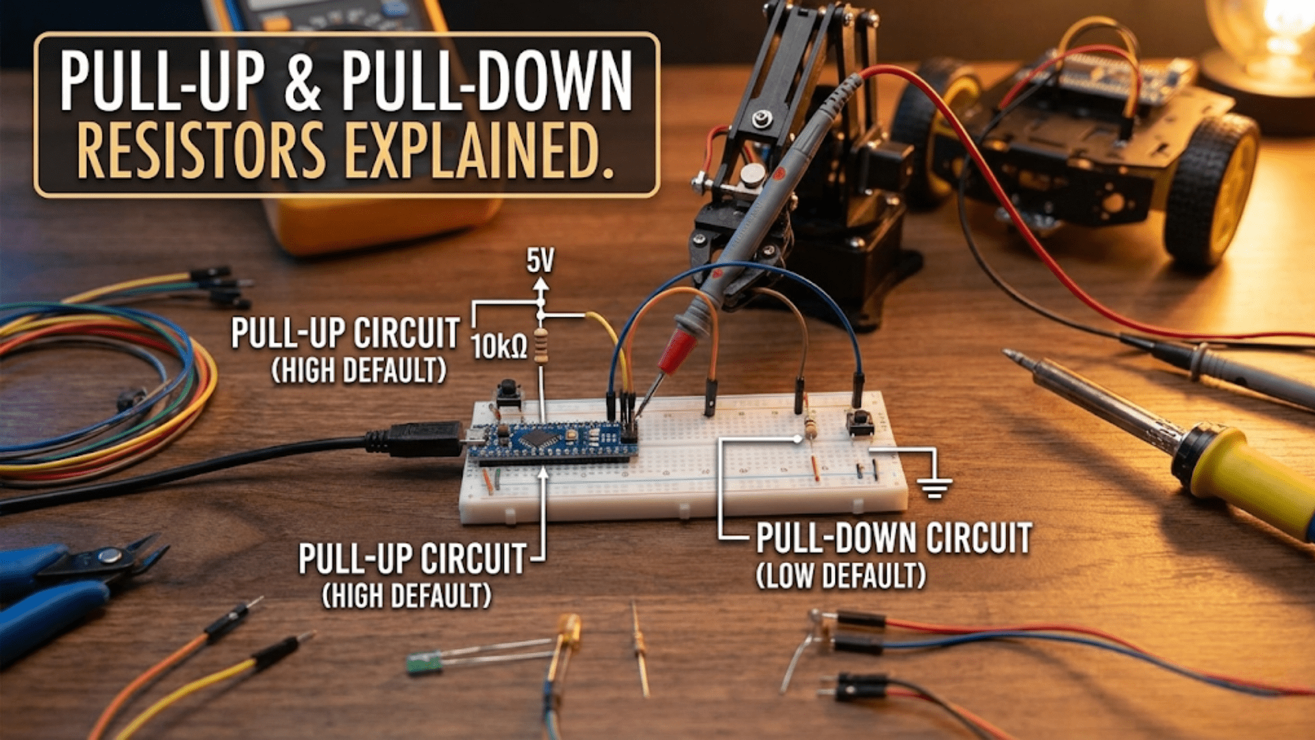
Switch 0 (LSB) → Pin 12 (A) with 10kΩ pull-up to VCC (switch shorts to GND when pressed)
Switch 1 → Pin 13 (B)
...
Switch 7 (MSB) → Pin 7 (H)
MCU GPIO → PL̅ (Pin 1)   [load strobe]
MCU GPIO → CP (Pin 2)    [shift clock]
MCU GPIO ← QH (Pin 10)  [serial data out]
CE̅ (Pin 15) → GND
DS (Pin 11) → GND
VCC (Pin 16) → 5V
GND (Pin 9) → GND
100nF decoupling between VCC and GNDReading code:
const int PL_PIN  = 7;   // Parallel load (active-LOW)
const int CP_PIN  = 6;   // Clock
const int QH_PIN  = 5;   // Serial output

uint8_t read165() {
  // 1. Pulse PL̅ LOW to load parallel inputs
  digitalWrite(PL_PIN, LOW);
  delayMicroseconds(1);         // Hold LOW for at least one setup time
  digitalWrite(PL_PIN, HIGH);   // Return HIGH — now in shift mode

  // 2. Read 8 bits, MSB first (H is first out after load)
  uint8_t result = 0;
  for (int i = 7; i >= 0; i--) {
    result |= (digitalRead(QH_PIN) << i);
    // Clock to shift next bit
    digitalWrite(CP_PIN, HIGH);
    delayMicroseconds(1);
    digitalWrite(CP_PIN, LOW);
    delayMicroseconds(1);
  }
  return result;
}After read165(), result bit 7 corresponds to switch H, bit 0 to switch A. A HIGH bit means the switch is open (pull-up holds high); LOW means the switch is pressed (shorted to GND).
Note on first bit: After loading (PL̅ pulse), the H bit is already present at QH before the first clock edge. The loop reads QH first, then clocks to advance to G, then reads G, and so on. The code above reads H first (i=7), then pulses CP to shift, then reads G (i=6) — correct.
Chaining 74HC165s for More Inputs
Connect QH of the first chip to DS (pin 11) of the second chip. Share CP and PL̅ between all chips:
Switch set 1 → [74HC165 #1] → QH → DS → [74HC165 #2] → QH → MCU
MCU → PL̅ → both chips
MCU → CP → both chipsAfter loading (PL̅ pulse), both registers are loaded. Read 16 bits serially: chip #2’s H bit comes out first, then its G…A bits, then chip #1’s H…A bits. Each additional chip adds 8 more inputs.
Special-Purpose Shift Register ICs
74HC594 — 74HC595 with Additional Register Clear
Like the 74HC595 but adds a separate active-LOW output register clear (RCLR̅). Allows clearing all outputs to zero without shifting in zeros. Useful when a fast guaranteed-zero output state is needed independently of the shift sequence.
74HC299 — Universal 8-Bit Shift Register
A versatile IC that supports all four modes (SIPO, PISO, SISO, PIPO) selected by two mode control inputs (S0, S1). Can shift left or right, load parallel data, and hold. Used in arithmetic logic units and data path applications where bidirectional shifting is needed.
74HC166 — Parallel Load Shift Register (Alternative to 74HC165)
An 8-bit shift register with synchronous parallel load, synchronous clear, clock enable, and serial input. Shifts data toward QH on each clock. Similar to 74HC165 but with different timing and control structure. Preferred in some synchronous designs because all operations (load, shift, clear) are clock-synchronous.
CD4094 — CMOS 8-Bit Shift and Store Register
CMOS equivalent of 74HC595 operation with wider supply range (3V–18V). Used in higher-voltage systems or where 12V operation is needed.
Shift Register Timing Analysis
Maximum Clock Frequency
For a 74HC595:
- Setup time (SER before SRCLK↑): t_su = 5ns
- Propagation delay SRCLK to QH’ (for chain): t_pCLK-Q ≈ 14ns
- Maximum SRCLK frequency: f_max = 1 / (t_pCLK-Q + t_su) = 1 / 19ns ≈ 52MHz (for single IC)
In practice, at 5V with proper decoupling, 74HC595 and 74HC165 operate reliably at 25MHz with a single IC. With multiple chained ICs, reduce frequency proportionally to account for QH’ propagation accumulation:
f_max_chain = 1 / (N × t_pQH' + t_su_last)For N=4 chips: f_max = 1/(4×14ns + 5ns) = 1/61ns ≈ 16MHz. Well within Arduino SPI’s 8MHz maximum.
Latency
Loading N bits into a SIPO register requires N clock cycles. At 1MHz clock: 8 bits = 8µs, 16 bits = 16µs, 32 bits = 32µs. At 8MHz: 8 bits = 1µs, 32 bits = 4µs. Typically negligible for LED driving or button reading applications.
Complete Design Examples
Design Example 1: 16-LED Bar Graph Driver
Application: Drive 16 individual LEDs from an Arduino Uno using only 3 pins. Each LED independently controllable. Display a bar graph, binary number, or pattern.
Components:
- 2× 74HC595
- 16× LEDs
- 16× 470Ω resistors
- 2× 100nF decoupling capacitors
- Arduino Uno
Wiring:
Arduino pin 11 (MOSI) → SER of 74HC595 #1 (pin 14)
Arduino pin 13 (SCK)  → SRCLK of both 74HC595s (pin 11)
Arduino pin 10 (SS)   → RCLK of both 74HC595s (pin 12) [repurposed as latch]
74HC595 #1 pin 9 (QH') → SER of 74HC595 #2 (pin 14)
All SRCLR̅ (pin 10) → VCC
All OE̅ (pin 13) → GND
LEDs 0-7:  QA-QH of 74HC595 #1 → 470Ω → LED → GND
LEDs 8-15: QA-QH of 74HC595 #2 → 470Ω → LED → GNDCurrent per LED: (5V − 2V) / 470Ω = 6.4mA — within 74HC595 output drive (35mA per pin maximum).
Maximum simultaneous LEDs on: 74HC595 total supply current limit is 70mA. At 6.4mA per LED: 70/6.4 ≈ 10 LEDs maximum on simultaneously per IC. If all 8 need to be on simultaneously, use 680Ω resistors (4.4mA each: 4.4 × 8 = 35mA — safely within one IC’s limit).
Complete Arduino code:
#include <SPI.h>

const int LATCH_PIN = 10;

void setup() {
  pinMode(LATCH_PIN, OUTPUT);
  SPI.begin();
  SPI.beginTransaction(SPISettings(8000000, MSBFIRST, SPI_MODE0));
  setLEDs(0, 0);  // All off
}

// leds_high: pattern for LEDs 15-8, leds_low: pattern for LEDs 7-0
void setLEDs(uint8_t leds_high, uint8_t leds_low) {
  digitalWrite(LATCH_PIN, LOW);
  SPI.transfer(leds_high);  // Goes to 74HC595 #2 (LEDs 8-15)
  SPI.transfer(leds_low);   // Goes to 74HC595 #1 (LEDs 0-7)
  digitalWrite(LATCH_PIN, HIGH);
  digitalWrite(LATCH_PIN, LOW);
}

void loop() {
  // Chase pattern across all 16 LEDs
  for (int i = 0; i < 16; i++) {
    uint16_t pattern = 1 << i;
    setLEDs((pattern >> 8) & 0xFF, pattern & 0xFF);
    delay(60);
  }

  // Binary count 0-65535
  for (uint16_t count = 0; count < 256; count++) {
    setLEDs(0, count);
    delay(10);
  }
}Design Example 2: 16-Button Keypad Scanner
Application: Read 16 pushbuttons (arranged as a 4×4 matrix of individual switches, each with pull-up) using only 2 MCU pins. Report which buttons are pressed.
Components:
- 2× 74HC165
- 16× push buttons
- 16× 10kΩ pull-up resistors
- Arduino
Wiring:
Arduino pin 7 → PL̅ of both 74HC165s (pin 1)
Arduino pin 6 → CP of both 74HC165s (pin 2)
74HC165 #1 pin 10 (QH) → DS of 74HC165 #2 (pin 11)
74HC165 #2 pin 10 (QH) → Arduino pin 5

All CE̅ (pin 15) → GND
74HC165 #1 DS (pin 11) → GND (no further input from left)

Buttons 0-7:  Each between one of 74HC165 #1 inputs (A-H) and GND
             Pull-up: 10kΩ from each input to VCC
Buttons 8-15: Each between 74HC165 #2 inputs (A-H) and GND
Pull-up: 10kΩ from each input to VCCReading code:
const int PL_PIN = 7;
const int CP_PIN = 6;
const int QH_PIN = 5;

uint16_t readButtons() {
  // Load parallel inputs
  digitalWrite(PL_PIN, LOW);
  delayMicroseconds(1);
  digitalWrite(PL_PIN, HIGH);

  uint16_t result = 0;
  // 16 bits: chip #2 bits come out first (bits 15-8), then chip #1 (bits 7-0)
  for (int i = 15; i >= 0; i--) {
    result |= ((uint16_t)digitalRead(QH_PIN) << i);
    digitalWrite(CP_PIN, HIGH);
    delayMicroseconds(1);
    digitalWrite(CP_PIN, LOW);
    delayMicroseconds(1);
  }
  return result;  // Bit LOW = button pressed (pull-up + switch to GND)
}

void loop() {
  uint16_t buttons = readButtons();
  uint16_t pressed = ~buttons;  // Invert: HIGH = pressed (active-HIGH logic)

  for (int i = 0; i < 16; i++) {
    if (pressed & (1 << i)) {
      Serial.print("Button ");
      Serial.print(i);
      Serial.println(" pressed");
    }
  }
  delay(50);  // 20Hz scan rate — fast enough for any button press
}Design Example 3: Four-Digit Seven-Segment Display with 74HC595
Application: Display a 4-digit number (0000–9999) on four common-cathode seven-segment displays using two 74HC595s and 4 transistors for digit selection. Multiplexed display — one digit on at a time, cycling fast enough to appear simultaneously on (persistence of vision at >50Hz).
Architecture:
One 74HC595 drives the 7 segment lines (a–g) plus one decimal point (dp) = 8 outputs total. Four NPN transistors (driven by 4 MCU GPIO pins) select which digit’s common cathode is grounded (enabling that digit).
Cycle: Enable digit 0, send segments for digit 0’s character → wait ~2ms → enable digit 1, send segments for digit 1 → wait ~2ms → … → repeat. At 4 digits × 2ms each = 8ms total cycle = 125Hz refresh. Well above 50Hz persistence-of-vision threshold.
Segment encoding for digits 0–9 (common-cathode, segments a=bit0, b=bit1, c=bit2, d=bit3, e=bit4, f=bit5, g=bit6):
const uint8_t digit_segments[10] = {
  0b00111111,  // 0: a,b,c,d,e,f
  0b00000110,  // 1: b,c
  0b01011011,  // 2: a,b,d,e,g
  0b01001111,  // 3: a,b,c,d,g
  0b01100110,  // 4: b,c,f,g
  0b01101101,  // 5: a,c,d,f,g
  0b01111101,  // 6: a,c,d,e,f,g
  0b00000111,  // 7: a,b,c
  0b01111111,  // 8: all segments
  0b01101111   // 9: a,b,c,d,f,g
};Display code:
#include <SPI.h>

const int LATCH_PIN = 10;
const int DIGIT_PINS[4] = {2, 3, 4, 5};  // NPN base pins for digits 0-3

void setup() {
  SPI.begin();
  SPI.beginTransaction(SPISettings(4000000, MSBFIRST, SPI_MODE0));
  pinMode(LATCH_PIN, OUTPUT);
  for (int i = 0; i < 4; i++) {
    pinMode(DIGIT_PINS[i], OUTPUT);
    digitalWrite(DIGIT_PINS[i], LOW);  // All digits off initially
  }
}

void sendSegments(uint8_t segments) {
  digitalWrite(LATCH_PIN, LOW);
  SPI.transfer(segments);
  digitalWrite(LATCH_PIN, HIGH);
  digitalWrite(LATCH_PIN, LOW);
}

void displayNumber(uint16_t number) {
  int digits[4];
  digits[3] = number % 10;
  digits[2] = (number / 10) % 10;
  digits[1] = (number / 100) % 10;
  digits[0] = number / 1000;

  for (int d = 0; d < 4; d++) {
    // Enable this digit's transistor
    digitalWrite(DIGIT_PINS[d], HIGH);
    // Send segment pattern
    sendSegments(digit_segments[digits[d]]);
    // Hold for 2ms (each digit visible for 2ms out of 8ms = 25% duty cycle)
    delay(2);
    // Turn off this digit before switching to next (prevents ghosting)
    sendSegments(0x00);
    digitalWrite(DIGIT_PINS[d], LOW);
  }
}

void loop() {
  for (uint16_t i = 0; i < 10000; i++) {
    // Display each number for ~80ms (10 refresh cycles × 8ms)
    for (int r = 0; r < 10; r++) {
      displayNumber(i);
    }
  }
}Ghost prevention: Setting segments to 0x00 before switching the digit select prevents “ghosting” — where segment drive from digit N briefly illuminates digit N+1 during the transition. The blank segment period is short (a few microseconds of SPI transfer time) and not visible.
Design Example 4: SPI Peripheral Expansion — MCP23S08
Application: Expand a microcontroller to 8 additional GPIO pins using the MCP23S08 SPI I/O expander. The MCP23S08 contains an 8-bit parallel I/O port accessible over SPI — it is essentially a shift register with register-addressable configuration and I/O functions.
While the MCP23S08 is not a pure shift register, understanding it reinforces shift register concepts and shows how the pattern scales to full I/O expansion chips.
SPI communication with MCP23S08:
#include <SPI.h>

const int CS_PIN = 10;
const byte MCP23S08_ADDR = 0x40;  // Address with A0=A1=0

// MCP23S08 register addresses
const byte IODIR   = 0x00;  // I/O direction (1=input, 0=output)
const byte IPOL    = 0x01;  // Input polarity
const byte GPPU    = 0x06;  // Pull-up enable
const byte GPIO_REG = 0x09; // GPIO port

void mcp_write(byte reg, byte data) {
  SPI.beginTransaction(SPISettings(10000000, MSBFIRST, SPI_MODE0));
  digitalWrite(CS_PIN, LOW);
  SPI.transfer(MCP23S08_ADDR | 0x00);  // Write command
  SPI.transfer(reg);
  SPI.transfer(data);
  digitalWrite(CS_PIN, HIGH);
  SPI.endTransaction();
}

byte mcp_read(byte reg) {
  SPI.beginTransaction(SPISettings(10000000, MSBFIRST, SPI_MODE0));
  digitalWrite(CS_PIN, LOW);
  SPI.transfer(MCP23S08_ADDR | 0x01);  // Read command
  SPI.transfer(reg);
  byte result = SPI.transfer(0x00);    // Dummy byte to clock data out
  digitalWrite(CS_PIN, HIGH);
  SPI.endTransaction();
  return result;
}

void setup() {
  pinMode(CS_PIN, OUTPUT);
  digitalWrite(CS_PIN, HIGH);
  SPI.begin();

  // Configure all 8 pins as outputs
  mcp_write(IODIR, 0x00);   // All outputs
  mcp_write(GPIO_REG, 0x00); // All LOW initially
}

void loop() {
  // Knight Rider pattern on 8 LEDs connected to MCP23S08 GP0-GP7
  for (int i = 0; i < 8; i++) {
    mcp_write(GPIO_REG, 1 << i);
    delay(80);
  }
  for (int i = 6; i >= 1; i--) {
    mcp_write(GPIO_REG, 1 << i);
    delay(80);
  }
}This demonstrates that SPI communication is fundamentally a shift register operation: each SPI.transfer() shifts 8 bits from the microcontroller into the peripheral (and simultaneously shifts 8 bits back from the peripheral to the microcontroller — full-duplex shift registers operating in both directions simultaneously).
Design Example 5: Shift Register Ring Oscillator and LFSR
Application: Use a 74HC595 as a Linear Feedback Shift Register (LFSR) to generate pseudo-random binary sequences, and separately as a ring counter for LED chasing patterns — demonstrating shift registers in feedback configurations.
Part A — Ring Counter from 74HC595:
Initialize the 74HC595 with exactly one ‘1’ bit (e.g., 0b00000001). Connect the serial output QH’ back to SER input. With SRCLK running and RCLK pulsed each cycle, the single ‘1’ bit circulates:
After 1 clock: 0b00000010 (LED 1 lights)
After 2 clocks: 0b00000100 (LED 2 lights)
...
After 7 clocks: 0b10000000 (LED 7 lights)
After 8 clocks: 0b00000001 (LED 0 lights again)A chasing LED pattern — the ‘1’ bit circulates at the clock frequency. With an Arduino providing the clock and latch at 20Hz, the chase appears smooth to the eye.
// Ring counter using 74HC595 with QH' fed back to SER
uint8_t ring = 0b00000001;  // Starting pattern: one LED on

void loop() {
  // Write current pattern
  sendTo595(ring);
  delay(50);  // 20Hz update rate

  // Rotate left: MSB wraps to LSB
  ring = (ring << 1) | (ring >> 7);
}Part B — 4-bit LFSR using flip-flops:
Using D flip-flops with XOR feedback, implement a maximal-length 4-bit LFSR (taps at positions 4 and 3 — output Q3 XOR Q2 feeds D0):
D0 = Q3 XOR Q2     (feedback from taps 4 and 3)
D1 = Q0
D2 = Q1
D3 = Q2The sequence cycles through all 15 non-zero 4-bit states before repeating. With a 74HC74 (two flip-flops) for Q0 and Q1, a second 74HC74 for Q2 and Q3, and one gate from a 74HC86 for the XOR:
// Software LFSR simulation (also verifies hardware behavior)
uint8_t lfsr = 0b0001;  // Non-zero start state

uint8_t lfsr_step(uint8_t state) {
  uint8_t feedback = ((state >> 3) ^ (state >> 2)) & 1;  // XOR of bits 3 and 2
  return ((state << 1) | feedback) & 0x0F;  // Shift left, insert feedback at bit 0
}

void loop() {
  lfsr = lfsr_step(lfsr);
  // Display lfsr on 4 LEDs...
  // Sequence: 1,2,4,9,3,6,13,11,7,15,14,12,8,1... (15 unique states)
  delay(100);
}Applications of LFSRs: Pseudo-random test pattern generation, spread-spectrum clock dithering to reduce EMI, CRC (cyclic redundancy check) error detection, stream cipher encryption key generation. Hardware LFSRs run at full clock frequency — a 74HC shift register LFSR generates pseudo-random bits at 50MHz+ rates, far faster than software pseudo-random generation.
Troubleshooting Shift Register Circuits
All outputs stuck HIGH or stuck LOW after power-up: OE̅ (pin 13) is floating. OE̅ = HIGH puts all outputs in tri-state (high-impedance), which may appear as HIGH or LOW depending on pull-up/pull-down conditions. Tie OE̅ directly to GND for always-enabled outputs.
Outputs change with every SRCLK pulse instead of waiting for RCLK: OE̅ is tied to GND and RCLK is connected to SRCLK (same pin). The storage register is being updated on every shift clock. These must be separate signals: SRCLK only shifts data through the shift register; RCLK separately latches the shift register to the output register.
First bit is wrong; remaining 7 bits are correct: Setup time violation. SER data is not stable before the first SRCLK rising edge. Ensure data is set before the clock rises. In software bit-bang: set SER pin, add a brief delay, THEN raise SRCLK. In SPI: the SPI peripheral handles timing automatically — no issue.
Chained 74HC595: last chip’s outputs are wrong: The chain length exceeds the timing margin at the current SPI clock rate. Each QH’ propagation adds ~14ns. Reduce SPI clock frequency or add a small RC delay at each QH’ connection to ensure signal integrity.
74HC165 reads all zeros or all ones regardless of switch state: PL̅ is not being pulsed LOW before reading. Without the load pulse, the shift register retains its old contents. The load pulse must be a genuine LOW pulse (≥ 20ns wide) before each read sequence. Alternatively, PL̅ may be floating HIGH (correct) but CE̅ (pin 15) is floating HIGH — tie CE̅ to GND.
Display ghosting on multiplexed 7-segment display: Segment data from the previous digit is briefly visible on the new digit during the switch. Between digit selections: blank all segments first (send 0x00), then switch the digit select transistor, then send the new segment pattern. The blanking period need only be a few microseconds.
Summary
Shift registers are chains of D flip-flops where each Q output drives the next D input, all sharing a common clock. Each clock edge shifts all data one position along the chain. The four configurations — SIPO (serial-in parallel-out), PISO (parallel-in serial-out), SISO (serial-in serial-out), and PIPO (parallel-in parallel-out) — handle the full range of serial/parallel conversion requirements.
The 74HC595 (SIPO with output latch) is the standard I/O expansion IC: 3 MCU pins control 8 outputs; daisy-chain N chips for 8N outputs from the same 3 pins. Its separate shift register and storage register ensure outputs remain stable during loading — no glitches on the output lines while data shifts in. The 74HC165 (PISO) is its complement: 3 MCU pins read 8 parallel inputs, with N chips chained for 8N inputs.
Both ICs are compatible with hardware SPI peripherals, enabling fast (up to 8MHz typical) data transfers that load 8 bits in about 1µs rather than 16µs for bit-banging. Maximum reliable clock frequency for chained ICs is approximately 1/(N × 14ns + 5ns), where N is the chain length.
The five design examples — 16-LED bar graph driver, 16-button keypad scanner, four-digit multiplexed seven-segment display, SPI I/O expander interface, and LFSR/ring-counter applications — span the breadth of practical shift register use in real designs.