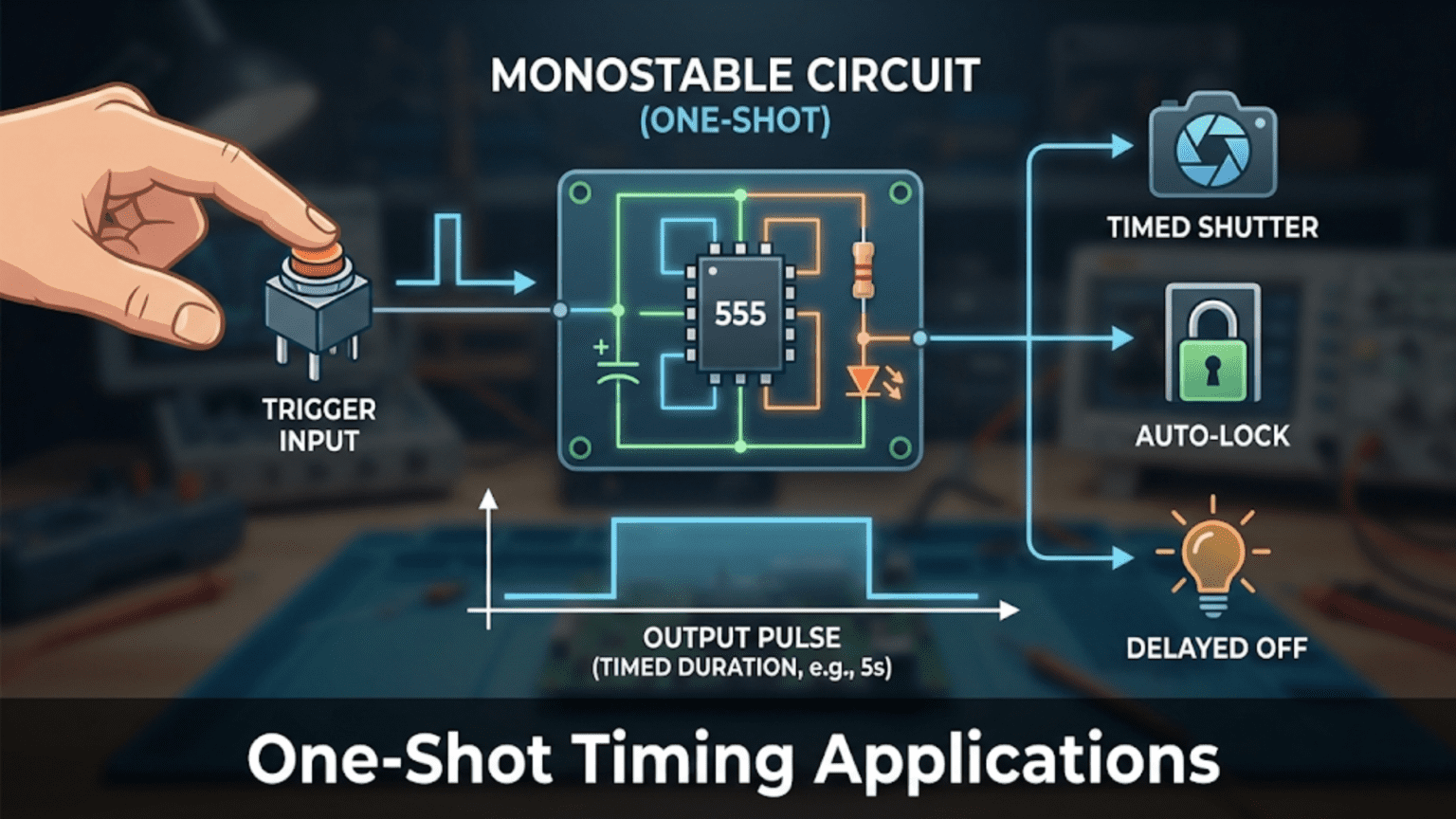
A monostable circuit — also called a one-shot timer — is a circuit with one stable resting state that produces a single output pulse of fixed duration each time it receives a trigger signal. Using a 555 timer IC in monostable mode, you can generate precise timing pulses ranging from microseconds to hours simply by choosing appropriate resistor and capacitor values, making it ideal for switch debouncing, time delays, pulse stretching, and automatic shutoff applications.
Introduction: One Trigger, One Pulse, Back to Rest
Imagine a light that turns on when you press a button and automatically turns off after exactly 30 seconds, no matter how long you hold the button or how many times you press it during that 30-second window. Or a door alarm that sounds for exactly 5 seconds every time the door opens, regardless of how quickly or slowly the door moves. Or a camera flash that fires once with a precise exposure duration when triggered by a sensor.
All of these behaviors share a common pattern: one trigger event produces one output pulse of defined length, and then the circuit returns to its resting state. This is the essence of the monostable circuit.
The word “monostable” breaks down into “mono” (one) and “stable” (steady state). Unlike the astable circuit that has no stable state and oscillates continuously, or the bistable circuit that has two stable states and stays in whichever one it was last put into, the monostable circuit has exactly one stable state — its resting, idle condition. When triggered, it briefly enters an unstable active state, generates an output pulse for a controlled duration, and then automatically returns to its single stable resting state.
The 555 timer IC in monostable mode is the most common and practical implementation of this concept. With just one resistor, one capacitor, and the chip itself, you can generate output pulses from a few microseconds to several hours with reasonable accuracy. The timing depends only on the RC values — not on the supply voltage, not on the trigger signal duration (within limits), not on the load connected to the output.
This article covers the monostable 555 circuit thoroughly: how it works internally, how to calculate timing components, the critical requirements for the trigger signal, what happens when you retrigger during an active pulse, how to extend the circuit for more complex applications, and a collection of detailed practical projects that demonstrate one-shot timing in real-world contexts. Whether you’re debouncing a noisy switch, creating a time-delay relay, stretching a narrow pulse to a usable width, or building a missing pulse detector, the monostable 555 circuit provides a reliable, low-cost solution.
Internal Operation: What Happens Inside the 555 in Monostable Mode
Understanding the internal mechanism is the foundation for using the circuit correctly. Many monostable circuit problems — triggers that don’t work, outputs that stay high permanently, pulses that end too early — trace directly to misunderstanding how the chip processes signals internally.
The Idle (Stable) State
When the monostable circuit is at rest with no active timing cycle:
- The output (pin 3) is LOW
- The internal discharge transistor is ON, connecting pin 7 to ground through the transistor
- The timing capacitor C1 (connected between pin 6/7 and ground) is held discharged at approximately 0V
- Pin 2 (TRIGGER) is held HIGH — above 1/3 VCC — by a pull-up resistor connected to VCC
- The internal flip-flop is in the reset state
The circuit sits patiently in this condition indefinitely, consuming minimal current (typically 3–15mA for the NE555, depending on supply voltage).
Triggering: Starting the Pulse
The monostable circuit triggers when pin 2 (TRIGGER) is pulled LOW — specifically, when it drops below 1/3 VCC. At that moment:
- The trigger comparator fires, detecting that pin 2 is below the 1/3 VCC threshold
- The comparator output sets the internal flip-flop
- The flip-flop switches state: output (pin 3) goes HIGH, discharge transistor turns OFF
- With the discharge transistor off, pin 7 is no longer connected to ground
- The timing capacitor C1 begins charging through R1 toward VCC
- The trigger pulse can now go back HIGH — the timing continues regardless
This is an important point: the trigger only needs to drop below 1/3 VCC briefly to initiate the timing cycle. Once the flip-flop is set, the trigger input is irrelevant until the current timing cycle ends and the circuit returns to idle.
The Timing Phase: Capacitor Charging
During the timing phase:
- Output is HIGH
- C1 charges through R1 following the exponential charging curve: V(t) = VCC × (1 – e^(-t/R1C1))
- Pin 6 (THRESHOLD) monitors the capacitor voltage
- Pin 2 (TRIGGER) is ignored — changes on this pin have no effect
The charging continues until the capacitor voltage reaches 2/3 VCC.
End of Timing: Returning to Idle
When C1 reaches 2/3 VCC:
- The threshold comparator fires, detecting that pin 6 has exceeded 2/3 VCC
- The comparator output resets the internal flip-flop
- The flip-flop switches back: output (pin 3) goes LOW, discharge transistor turns ON
- The discharge transistor connects pin 7 to ground, rapidly discharging C1 through the transistor (no external resistor in the discharge path)
- C1 discharges almost instantly — limited only by the transistor’s saturation resistance (~10–50Ω) and any wiring resistance
- The circuit returns to its idle state, ready for the next trigger
The output pulse duration is the time from triggering to the capacitor reaching 2/3 VCC — determined entirely by R1 and C1.
The Reset Pin: Immediate Termination
Pin 4 (RESET) provides an emergency stop. Pulling pin 4 LOW at any point immediately resets the flip-flop, regardless of the timing state. The output goes LOW, the discharge transistor turns ON, and C1 discharges. The circuit returns to idle even if a timing cycle was in progress.
This is useful for abort conditions — canceling a timed delay if a safety condition is detected, for example. When not using the reset function, pin 4 must be connected firmly to VCC. A floating reset pin is one of the most common causes of erratic monostable behavior.
The Timing Formula: Calculating Pulse Duration
The monostable pulse duration derives from the RC capacitor charging equation. When C1 charges from 0V toward VCC, the time to reach 2/3 VCC is:
T = R1 × C1 × ln(3) = R1 × C1 × 1.0986... ≈ 1.1 × R1 × C1Where:
- T = pulse duration in seconds
- R1 = timing resistor in ohms
- C1 = timing capacitor in farads
- ln(3) ≈ 1.0986 (the natural logarithm of 3)
The approximation T ≈ 1.1 × R1 × C1 is accurate to within 0.1% and is universally used in practice.
Rearranging for component selection:
R1 = T / (1.1 × C1)
C1 = T / (1.1 × R1)Derivation for the Curious
The capacitor charges from 0V (fully discharged) toward VCC with time constant τ = R1 × C1:
V(t) = VCC × (1 - e^(-t/R1C1))Setting V(t) = 2/3 VCC and solving for t:
2/3 × VCC = VCC × (1 - e^(-T/R1C1))
2/3 = 1 - e^(-T/R1C1)
e^(-T/R1C1) = 1/3
-T/R1C1 = ln(1/3) = -ln(3)
T = R1 × C1 × ln(3) ≈ 1.0986 × R1 × C1The factor of ln(3) — approximately 1.1 — is what makes the monostable formula slightly different from the astable formula (which uses ln(2) ≈ 0.693). The monostable capacitor starts at 0V and charges to 2/3 VCC; the astable capacitor starts at 1/3 VCC and charges to 2/3 VCC (a smaller swing requiring less time).
Component Selection Guide
| Target Pulse Duration | Choose C1 | Calculate R1 |
|---|---|---|
| 1µs – 100µs | 1nF – 10nF | 91Ω – 9.1MΩ |
| 100µs – 10ms | 10nF – 100nF | 91Ω – 9.1MΩ |
| 10ms – 1s | 100nF – 10µF | 910Ω – 91kΩ |
| 1s – 100s | 10µF – 100µF | 91kΩ – 9.1MΩ |
| 100s – 3 hours | 100µF – 1000µF | 91kΩ – 9.1MΩ |
Practical resistor limits: Keep R1 between 1kΩ and 10MΩ. Below 1kΩ, current demand during timing may affect supply voltage. Above 10MΩ, capacitor leakage current distorts timing significantly.
Practical capacitor advice: For pulse durations above about 1 second, you’ll need electrolytic capacitors. These have ±20% tolerance and significant leakage — expect timing accuracy of ±10–20% with electrolytics. For sub-second precision, use polyester film or ceramic C0G/NP0 capacitors (±1–5% tolerance) for ±2–5% timing accuracy.
Worked Examples
Example 1: 500ms one-shot pulse
Choose C1 = 10µF (electrolytic, adequate accuracy for most applications):
R1 = T / (1.1 × C1) = 0.5 / (1.1 × 10×10⁻⁶) = 0.5 / 0.000011 = 45,455Ω → use 47kΩVerify: T = 1.1 × 47,000 × 10×10⁻⁶ = 1.1 × 0.47 = 0.517 seconds ✓ (within 3.4% of 500ms)
Example 2: 10-second delay relay
Choose C1 = 100µF:
R1 = 10 / (1.1 × 100×10⁻⁶) = 10 / 0.00011 = 90,909Ω → use 91kΩ or 100kΩWith 100kΩ: T = 1.1 × 100,000 × 100×10⁻⁶ = 11 seconds (within 10% — acceptable with electrolytic)
Example 3: 1ms precision pulse for sensor timing
Choose C1 = 100nF (film capacitor for accuracy):
R1 = 0.001 / (1.1 × 100×10⁻⁹) = 0.001 / 0.00000011 = 9,091Ω → use 9.1kΩ or 10kΩWith 10kΩ: T = 1.1 × 10,000 × 100×10⁻⁹ = 1.1ms (within 10% — use precision 9.1kΩ for better accuracy)
Example 4: Variable timing with potentiometer
Replace R1 with a potentiometer (R_pot) in series with a minimum fixed resistor (R_min = 1kΩ):
T_min = 1.1 × R_min × C1        [potentiometer at 0]
T_max = 1.1 × (R_min + R_pot) × C1 [potentiometer at maximum]For a 1s–10s timer with C1 = 100µF:
- R_min = 1kΩ: T_min = 1.1 × 1000 × 100×10⁻⁶ = 0.11s
- R_pot = 100kΩ: T_max = 1.1 × 101,000 × 100×10⁻⁶ = 11.1s
A 100kΩ potentiometer with 1kΩ series resistor and 100µF capacitor gives a roughly 0.1s to 11s adjustable one-shot timer.
Critical Trigger Requirements
The trigger input is the most misunderstood aspect of monostable circuits. Getting it wrong causes the most common monostable failures.
Requirement 1: The Trigger Must Fall Below 1/3 VCC
The trigger comparator inside the 555 fires when pin 2 drops below 1/3 VCC. For a 9V supply, 1/3 VCC = 3V. For a 5V supply, 1/3 VCC = 1.67V.
If your trigger signal only drops to, say, 2V on a 5V supply, it might be close to the 1.67V threshold but may not reliably trigger due to noise or threshold tolerance. Ensure the trigger signal swings fully to GND (0V) for reliable triggering.
Requirement 2: The Trigger Must Be a Negative-Going Edge
The 555 monostable triggers on a falling edge — when pin 2 transitions from HIGH to LOW. A signal that is permanently low will not trigger additional pulses. The trigger must be high in the idle state and then pulled low to initiate each timing cycle.
This is why a pull-up resistor is essential: without it, pin 2 has no defined idle state voltage, and the circuit may trigger spontaneously from noise or capacitive coupling.
Requirement 3: The Trigger Should Return HIGH Before T Expires (Standard NE555)
Here is the most important and most often overlooked requirement: in the standard NE555, if the trigger signal remains below 1/3 VCC when the timing cycle ends, the output will NOT return low.
This happens because the threshold comparator is trying to reset the flip-flop (capacitor has charged to 2/3 VCC), but the trigger comparator is simultaneously trying to set it (pin 2 is still below 1/3 VCC). The trigger comparator wins — the flip-flop stays set, the output stays high, and the capacitor discharges and recharges repeatedly.
In practice this means: if you hold a button connected to pin 2 for longer than the timing period T, the output stays high until you release the button, then the timing period runs from the moment of release. This behavior can be intentional (making the timing period relative to button release rather than button press) but is often unexpected for beginners.
Solutions:
- Use a differentiation network (RC circuit) on the trigger input to convert a long button press into a short pulse (see Trigger Conditioning below)
- Use a CMOS 555 variant (LMC555, TLC555) which handles overlapping trigger and threshold conditions differently
- Use the RESET pin to force the output low if the trigger overstays its welcome
Trigger Conditioning: Converting Slow Signals to Short Pulses
A differentiation network converts a slow-changing or long trigger signal into a brief pulse suitable for the 555:
Components: 10kΩ resistor (R_d) and 10nF capacitor (C_d) in series between the trigger source and pin 2, with a 10kΩ pull-up resistor from pin 2 to VCC.
How it works: When the trigger source goes LOW, C_d initially passes the full voltage change through to pin 2, pulling it low. But C_d quickly charges through R_d, and pin 2 rises back toward VCC. The pulse width at pin 2 is approximately:
t_pulse ≈ R_d × C_d × ln(2) ≈ 0.693 × R_d × C_dWith 10kΩ and 10nF: t_pulse ≈ 0.693 × 10,000 × 10×10⁻⁹ = 69.3µs
This brief 69µs pulse reliably triggers the 555 regardless of how long the original trigger signal stays low. The trigger can be held low for hours without affecting the monostable output pulse duration.
Clipping diode: Add a 1N4148 diode from pin 2 to GND (anode to GND, cathode to pin 2). When the capacitor has charged and pin 2 rises above VCC, the diode clamps it to prevent excessive voltage on the trigger pin. Also prevents the positive spike that appears when the trigger signal goes back HIGH from accidentally retriggering the circuit.
Retriggering: What Happens During an Active Cycle
What happens if a new trigger arrives while a timing cycle is already in progress? The behavior depends on the 555 variant and circuit configuration.
Standard NE555: Non-Retriggerable
In the standard NE555 monostable circuit, a new trigger arriving while the output is already HIGH has no effect. The flip-flop is already set — setting it again doesn’t change anything. The timing cycle continues to its natural end, the output goes low, and the circuit is then ready for the next trigger.
This non-retriggerable behavior is often exactly what you want. For example, in a door alarm application, you don’t want each vibration during the alarm period to restart the 5-second alarm from scratch — you want the alarm to run for exactly 5 seconds from the first trigger, then stop.
Practical non-retriggerable monostable uses:
- Debouncing switches (ignore subsequent bounces after first trigger)
- Alarm hold (run alarm for fixed period regardless of repeated sensor triggers)
- Pulse stretching (convert any short pulse to a fixed-length pulse)
- Rate limiting (enforce minimum time between output activations)
Making a Retriggerable Monostable
Sometimes you want each new trigger to restart the timing cycle. For example, an automatic light that stays on as long as motion continues and turns off only after motion stops for 5 minutes — each detected motion restarts the 5-minute countdown.
Method 1: External reset and retrigger
Connect a logic gate (NAND or NOR) so that any new trigger simultaneously:
- Pulls pin 2 (TRIGGER) low via the trigger input path
- Pulls pin 4 (RESET) low briefly to cancel any running cycle
Then immediately releases both. The circuit resets and immediately retriggers — effectively restarting the timing from zero.
Method 2: Using dedicated retriggerable one-shot ICs
The 74HC123 and CD4528 are dedicated retriggerable monostable ICs that restart their timing on each incoming trigger pulse. These are more appropriate than modifying the 555 when retriggerable behavior is specifically required.
Method 3: Microcontroller-based timing
For complex retriggerable timing requirements, a microcontroller (even an inexpensive ATtiny85) handles retriggerable timing in software far more flexibly than analog circuits.
Complete Practical Circuit Projects
Project 1: Switch Debouncer
Mechanical switches bounce — when you press a button, the contacts open and close rapidly several times before settling. This produces multiple edges within a few milliseconds, causing digital circuits to register multiple “presses” from a single physical press.
The monostable solution: When the first falling edge arrives (button pressed), the 555 triggers and the output goes HIGH for a defined period — long enough for the bounce to end (typically 5–50ms) but short enough to be unnoticeable to the user. During this period, additional trigger edges are ignored (non-retriggerable behavior). The clean, single output pulse is what downstream logic sees.
Components:
- NE555
- R1 = 22kΩ (timing resistor)
- C1 = 1µF electrolytic (timing capacitor)
- R_pull = 10kΩ (pull-up on trigger input, pin 2)
- C2 = 10nF (pin 5 bypass)
- Momentary push button between pin 2 and GND
- 9V supply with decoupling capacitors
Timing calculation:
T = 1.1 × 22,000 × 1×10⁻⁶ = 24.2msA 24ms output pulse — long enough to outlast any mechanical bounce (which typically lasts 1–15ms), short enough to feel instantaneous to a human user.
Circuit connections:
- Pin 1 → GND
- Pin 2 → 10kΩ pull-up to VCC; push button from pin 2 to GND
- Pin 3 → Output to downstream logic
- Pin 4 → VCC
- Pin 5 → 10nF → GND
- Pin 6 → Pin 7 (tied together) → top of C1 → GND (negative)
- R1 from VCC to pin 7
- Pin 8 → VCC
How to use: Connect pin 3 output to the clock input of a flip-flop, counter, or microcontroller interrupt pin. The output produces a clean 24ms HIGH pulse for each button press, with no bounce pulses.
Project 2: Automatic Stairwell Light Timer (30-Second Hold)
A stairwell light turns on when a button is pressed and stays on for exactly 30 seconds, then turns off automatically — even if nobody presses the button again.
Components:
- NE555
- R1 = 300kΩ (or 270kΩ + trim pot for adjustment)
- C1 = 100µF electrolytic
- R_pull = 10kΩ (pin 2 pull-up)
- C2 = 10nF (pin 5 bypass)
- Momentary push button (pin 2 to GND)
- 5V relay module (coil driven from pin 3)
- 1N4007 flyback diode across relay coil
- 12V supply
Timing calculation:
T = 1.1 × 300,000 × 100×10⁻⁶ = 33 secondsClose enough to 30 seconds; fine-tune with the trim pot or adjust R1 to 270kΩ:
T = 1.1 × 270,000 × 100×10⁻⁶ = 29.7 seconds ✓Operation: Press the button momentarily. The relay energizes (connecting mains-powered light through the relay’s normally-open contacts), stays energized for 30 seconds, then releases. The relay isolates the high-voltage mains wiring from the low-voltage 555 circuit.
Safety note: The relay’s normally-open contacts can switch mains voltage (120V/240V AC) at appropriate current ratings. Always use a relay rated for the load current and voltage. Never connect mains voltage directly to the 555 circuit. If you’re not experienced with mains wiring, use a relay module with built-in optoisolation and have the mains connections reviewed by a qualified electrician.
Project 3: Pulse Stretcher / Width Expander
Some sensors and signal sources produce pulses that are too short for downstream circuits to reliably detect. An infrared sensor might output a 10µs pulse; a microcontroller’s interrupt might miss anything shorter than 100µs. The monostable 555 stretches these narrow pulses to any desired width.
Target: Convert 10µs input pulses to 1ms output pulses (100× stretch)
Components:
- NE555
- R1 = 9.1kΩ
- C1 = 100nF ceramic (film capacitor for accuracy)
- R_d = 1kΩ (differentiation resistor, input protection)
- C_d = 1nF (differentiation capacitor, forms input pulse conditioning network)
- D1 = 1N4148 (input clamp diode)
- C2 = 10nF (pin 5 bypass)
- 5V supply
Timing calculation:
T = 1.1 × 9,100 × 100×10⁻⁹ = 1.001ms ✓Input conditioning: The 1kΩ/1nF RC differentiation network on the input converts the sensor’s 10µs pulse into a brief edge-triggered impulse at pin 2. The 1N4148 clamp prevents pin 2 from going above VCC or excessively below GND.
Operation: Each 10µs input pulse produces a clean 1ms output pulse. The downstream circuit now has 100 times longer to detect each event. This circuit is used in sensor interfaces, communications signal processing, and logic level adapters.
Project 4: Missing Pulse Detector
This elegant application uses the non-retriggerable monostable in a clever way: when a regularly arriving signal is present, the circuit never times out; when the signal stops or slows, the timeout triggers an alarm.
Concept: An astable oscillator (or another signal source) continuously triggers the monostable with a period slightly shorter than the monostable’s timing period T. Under normal operation, each new trigger arrives before the previous timing cycle expires, restarting the cycle before it can complete. The output stays HIGH indefinitely.
Wait — we just said the standard NE555 is non-retriggerable. How does this work?
The trick: With a differentiation network, each trigger input creates a brief pulse at pin 2. Once the timing cycle completes (output goes LOW momentarily), it can be retriggered by the next incoming pulse. But if a pulse is missing — if the input signal stops — the timing cycle completes, the output goes LOW, and stays LOW until a new trigger arrives. This LOW output signals the missing pulse condition.
For this to work correctly: The monostable timing period T must be longer than the expected pulse interval by a safe margin (typically 20–50% longer). If expected pulses arrive every 100ms, set T = 120–150ms. This way, during normal operation, the output pulses briefly LOW between each retrigger and then goes HIGH again — or for clean operation, use a retriggerable configuration.
A cleaner implementation uses a retriggerable monostable (74HC123) instead of the 555, as the retriggerable device keeps the output continuously HIGH during normal signal arrival and outputs a clean LOW when signal is missing.
Practical applications:
- Heart rate monitor alarm (missing heartbeat triggers alert)
- Conveyor belt jam detector (missing product sensor pulse indicates jam)
- Motor rotation monitor (missing encoder pulse indicates stalled motor)
- Communication watchdog (missing data packet triggers error condition)
- Stepper motor stall detection (missing step pulse indicates mechanical problem)
Project 5: Touch-Activated Timer
The 555’s trigger input has very high input impedance — the internal comparator draws negligible current. This sensitivity allows the human body’s capacitance and resistance to directly trigger the monostable when a metal pad is touched.
Components:
- NE555
- R1 = 100kΩ (timing resistor for ~10 second pulse)
- C1 = 100µF
- R_pull = 10MΩ (very high value pull-up on trigger input)
- Touch pad: small piece of copper-clad board or metal foil connected to pin 2
- LED + 470Ω resistor from pin 3 to GND (output indicator)
- C2 = 10nF (pin 5 bypass)
- 9V battery supply
How it works: Pin 2 is held at approximately VCC by the 10MΩ pull-up. When a finger touches the metal pad connected to pin 2, the human body acts as a resistor to ground (~1MΩ to 10MΩ typical body resistance). The finger-body resistance forms a voltage divider with the 10MΩ pull-up, pulling pin 2 below 1/3 VCC and triggering the monostable. The output LED lights for approximately:
T = 1.1 × 100,000 × 100×10⁻⁶ = 11 secondsTouch the pad, the LED lights for 11 seconds, then turns off automatically. No mechanical switch needed.
Timing calculation:
T = 1.1 × R1 × C1 = 1.1 × 100,000 × 100×10⁻⁶ = 11 secondsSensitivity note: Sensitivity varies with body size, moisture, and contact area. In dry environments or with small contact pads, sensitivity may be insufficient. Increase R_pull to 22MΩ or increase the touch pad area for better sensitivity. In noisy electrical environments, stray interference may cause false triggers — add a 100pF capacitor from pin 2 to GND to filter high-frequency noise.
Timing Accuracy: Understanding and Improving It
The monostable 555’s timing accuracy depends on several factors that every practical designer should understand.
Component Tolerance
The timing formula T = 1.1 × R1 × C1 assumes exact component values. In practice:
Resistors: Standard ±5% tolerance resistors (E24 series, marked with gold band) introduce up to ±5% timing error. Precision ±1% resistors (E96 series, usually in SMD packages) reduce this to ±1%.
Capacitors: This is the dominant source of error. Electrolytic capacitors are typically ±20% tolerance — a 100µF capacitor could be anywhere from 80µF to 120µF. Ceramic capacitors vary dramatically by type:
- Z5U/Y5V ceramics: ±80%/−20% tolerance — essentially useless for timing
- X7R ceramics: ±10–15% tolerance — acceptable for rough timing
- C0G/NP0 ceramics: ±5% tolerance, minimal temperature coefficient — best for precision timing
- Polyester film capacitors: ±5–10% tolerance, stable — good general-purpose timing caps
- Polypropylene film: ±1–2.5% tolerance — excellent for precision timing
For a 30-second timer using a 100µF electrolytic (±20%) and 270kΩ ±5% resistor, the actual timing could range from:
T_min = 1.1 × 270,000 × 0.95 × 80×10⁻⁶ = 22.5 seconds
T_max = 1.1 × 270,000 × 1.05 × 120×10⁻⁶ = 37.5 secondsA 25-second spread on a 30-second target — ±25% accuracy. For non-critical applications (stairwell lights, buzzers) this is fine. For critical applications, use precision components or calibrate with a trim potentiometer.
Temperature Effects
The NE555’s internal voltage divider resistors have a temperature coefficient of approximately 50ppm/°C. Over a 50°C operating range (e.g., −10°C to +40°C), this causes approximately 0.25% timing variation — negligible for most applications.
Electrolytic capacitors change capacitance significantly with temperature — typically ±20% over the operating range. Combined with the already-large tolerance, this makes electrolytics unsuitable for precision timing across temperature ranges.
CMOS 555 variants (LMC555, ICM7555) generally have better temperature stability than the bipolar NE555 due to the more predictable properties of CMOS transistor thresholds.
Supply Voltage Independence
A key feature of the 555 monostable is its theoretical independence from supply voltage. Since the timing thresholds are set at 1/3 VCC and 2/3 VCC, and the capacitor charges from 0V toward VCC, the ratio that determines when timing ends (2/3 VCC) is the same fraction regardless of VCC’s actual value. If VCC drops from 9V to 8V, the thresholds change from 6V/3V to 5.33V/2.67V — and the capacitor still charges from 0V to 2/3 of the new VCC in the same time T = 1.1 × R1 × C1.
In practice, there’s a small supply voltage dependence due to the discharge transistor’s saturation voltage and the output stage’s behavior at different currents, but it’s typically less than 1% across the full VCC operating range.
Calibration with a Trim Potentiometer
For applications requiring reasonably precise timing without expensive precision components, replace the fixed R1 with a fixed resistor in series with a multi-turn trim potentiometer (cermet type for stability). A 10-turn 10kΩ trim pot allows fine adjustment of the timing period:
- Build the circuit with nominal components
- Connect a frequency counter or oscilloscope to measure the actual pulse width
- Adjust the trim pot until the measured pulse width matches the target
- Lock the trim pot with a small drop of nail varnish or glue to prevent vibration from changing the setting
This calibration approach achieves ±2–5% accuracy even with standard-tolerance electrolytics.
Advanced Monostable Configurations
Cascaded Monostables: Sequential Timing
Two monostable 555 circuits can be cascaded so that the end of the first pulse triggers the start of the second. Connect the output (pin 3) of the first 555 to the trigger input (pin 2) of the second 555 through a differentiation network. The falling edge at the end of the first pulse triggers the second timer.
Application example: Stage lighting control. Stage 1: house lights fade down (first monostable controls a relay for 5 seconds). At the end of 5 seconds, stage 2 automatically starts: stage lights fade up (second monostable controls a different relay for 8 seconds). No manual intervention needed.
Cascading depth: You can chain multiple monostables for multi-stage sequential timing. Three cascaded timers create a three-step automatic sequence.
Monostable + Astable Combination: Delayed Oscillation
Combine a monostable (555 #1) with an astable (555 #2) so that the oscillator only runs during the monostable’s output pulse. Connect the monostable’s output to the RESET pin (pin 4) of the astable circuit:
- When monostable output is LOW (idle): astable reset pin is LOW, oscillator is held off
- When monostable output is HIGH (triggered): astable reset pin is HIGH, oscillator runs freely
Application: A beeping alarm that activates for exactly 10 seconds when triggered, then silences automatically. The monostable controls the duration; the astable generates the beeping tone.
Long-Duration Timing: Extending Beyond RC Limits
For timing periods of hours or days, electrolytic capacitor leakage makes direct RC timing impractical. Better approaches:
Counter-based extension: Run a 555 astable at a higher frequency (say, 1Hz) and count its output pulses with a CMOS counter IC (CD4017, CD4060). The counter divides the frequency by 10, 100, or 1000, enabling hour-long periods with small, stable capacitors.
Real-time clock IC: For precise long-duration timing (hours to days), a dedicated RTC IC (DS1307, DS3231) with a crystal oscillator is more accurate and power-efficient than any RC approach.
Comparison: Monostable 555 vs. Other One-Shot Approaches
| Approach | Timing Range | Accuracy | Power | Complexity | Best For |
|---|---|---|---|---|---|
| 555 Monostable | 1µs – 100s | ±5–20% | Medium | Very low | General one-shot, prototyping |
| 74HC123 Retriggerable | 1µs – 100ms | ±5–10% | Low | Low | Retriggerable, faster recovery |
| RC + comparator | 1µs – 1000s | ±1–5% | Low | Medium | Precision analog timing |
| Microcontroller | Unlimited | ±0.01% (crystal) | Medium | High | Complex timing, programmable |
| RTC + counter | Minutes – days | ±0.001% | Very low | Medium | Long periods, battery operation |
| Crystal oscillator + counter | Any | ±0.005% | Low | Medium | Precision, communication |
The 555 monostable is the right choice when you need simple, reliable one-shot timing with minimal components, moderate accuracy (±5–20%), and timing periods from microseconds to a few hundred seconds. For longer periods, higher precision, or retriggerable behavior, the alternatives above offer advantages.
Troubleshooting Monostable Circuits
Problem: Output stays HIGH permanently after triggering
- Most likely cause: Trigger pin 2 is staying below 1/3 VCC after the timing cycle ends. The circuit can’t reset because the trigger comparator keeps the flip-flop set.
- Solution: Add trigger conditioning (differentiation RC network) to convert long trigger signals to brief pulses. Verify the trigger source returns HIGH after triggering.
Problem: No output pulse when triggered
- Check pin 4 (RESET) — must be HIGH. A floating or grounded RESET pin prevents any output.
- Verify trigger signal actually drops below 1/3 VCC — measure with a multimeter or oscilloscope.
- Check C1 polarity (electrolytic) — reversed polarity causes the capacitor to conduct rather than charge.
- Verify R1 is connected correctly — between VCC and pin 7 (not pin 6/2).
Problem: Pulse duration too short
- C1 value is lower than expected — measure actual capacitance.
- R1 value is lower than expected — measure with multimeter.
- Capacitor leakage — try a new capacitor or a different type (film vs. electrolytic).
Problem: Pulse duration too long
- C1 value higher than expected — electrolytic capacitors often exceed nominal value, especially when new.
- Stray capacitance at timing node — long breadboard wires or large copper areas add capacitance. Keep wiring short.
- Body capacitance — if you’re touching the circuit during measurement, your body adds capacitance. Use insulated tools when measuring.
Problem: Erratic triggering, false triggers
- Pin 2 floating without pull-up resistor — add 10kΩ pull-up to VCC.
- Electrical noise on trigger line — add 100pF capacitor from pin 2 to GND to filter high-frequency noise.
- Insufficient power supply decoupling — add 100nF ceramic + 10µF electrolytic close to the IC.
- Pin 5 not bypassed — add 10nF from pin 5 to GND.
Summary
The monostable 555 circuit is one of the most practically useful building blocks in electronics. Its operation is straightforward: a trigger on pin 2 sets the internal flip-flop, starting a timing cycle during which the output is HIGH; when the timing capacitor reaches 2/3 VCC, the flip-flop resets, ending the pulse and discharging the capacitor back to 0V. The pulse duration T = 1.1 × R1 × C1 depends only on the timing components, not on supply voltage, trigger duration, or output load.
Critical design points to remember: pin 4 (RESET) must be tied to VCC when not used; the trigger signal must return HIGH before the timing period ends in standard NE555 circuits; use a differentiation network for long or slow trigger signals; choose timing capacitors appropriate to the required accuracy (C0G/NP0 or film for precision, electrolytic for long periods where tolerance is acceptable).
The monostable 555 finds practical application in switch debouncing, time-delay relays, pulse stretching, touch sensors, missing pulse detection, sequential timing chains, and countless other one-shot timing needs. Its low cost, minimal component count, wide operating voltage range, and robust output drive capability make it a reliable choice for prototyping and production alike.