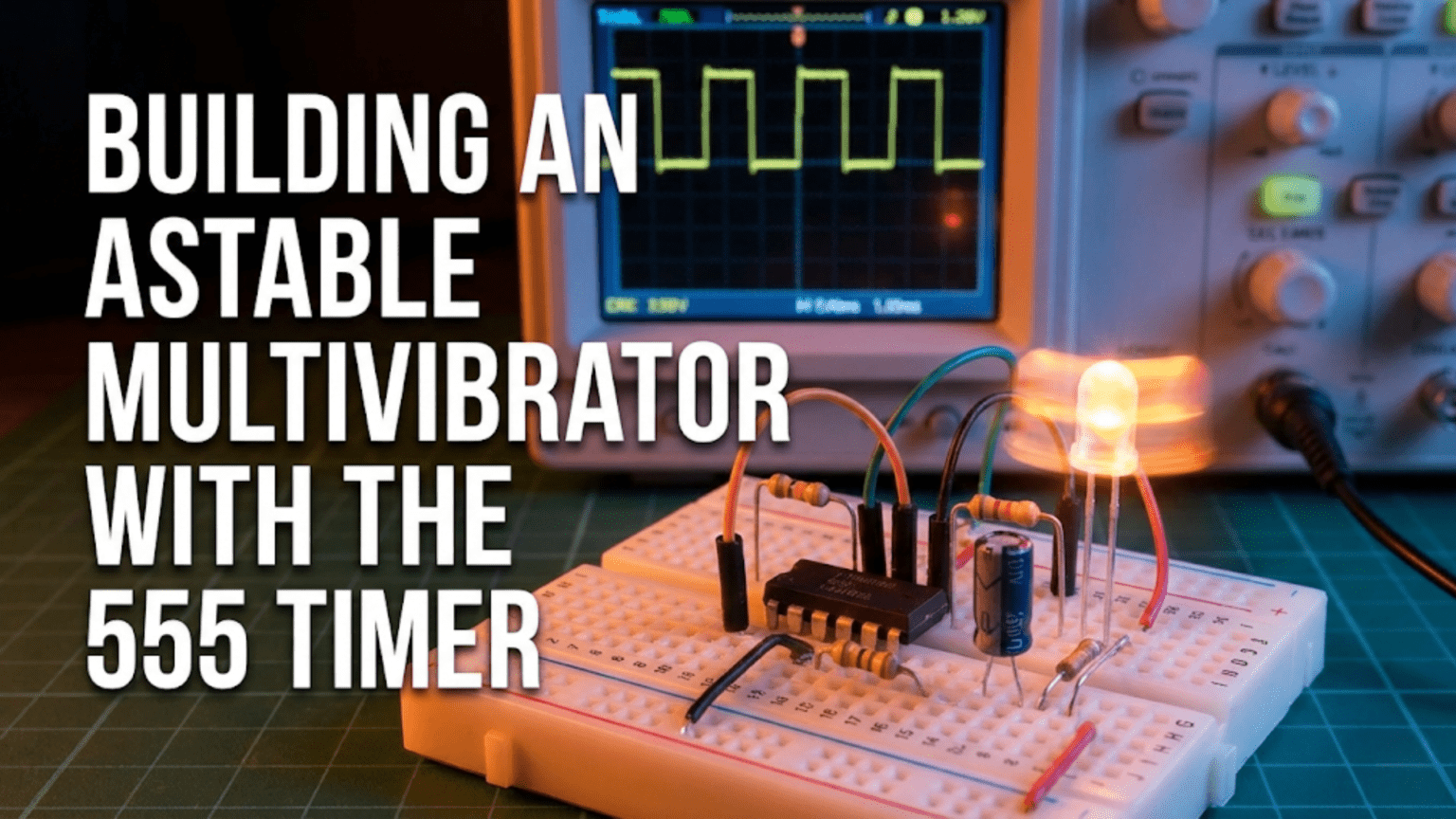
An astable multivibrator built with a 555 timer is a free-running oscillator circuit that continuously switches its output between high and low states without any external trigger. By connecting two resistors and a capacitor to the 555 timer IC, you can generate square waves with precisely controlled frequency and duty cycle for applications ranging from LED blinking to audio tone generation and clock signal production.
Introduction: The Circuit That Never Stops
Some circuits wait patiently for a signal before doing anything. Others do their work once and then go quiet. But the astable multivibrator is different, it never stops. Power it up, and it immediately begins oscillating, flipping its output between high and low in a relentless rhythm determined entirely by the values of two resistors and a capacitor.
The word “astable” comes from the Greek prefix “a-” meaning “without” combined with “stable” — literally, a circuit with no stable state. Unlike a bistable circuit that rests in one of two steady states, or a monostable circuit that has one resting state it returns to after being triggered, the astable circuit has no resting state at all. It perpetually cycles between high and low, high and low, forever.
The 555 timer IC makes building an astable multivibrator remarkably straightforward. With just two resistors, one capacitor, and the chip itself, you can generate square waves from a fraction of a hertz all the way to several hundred kilohertz. Change the resistor and capacitor values and you change the frequency. Adjust the ratio of the two resistors and you change the duty cycle — how long the output spends high compared to low.
This versatility makes the 555 astable circuit one of the most useful building blocks in all of electronics. Whether you need a clock signal for a digital circuit, a tone for a buzzer, a blinking rate for an indicator LED, a carrier frequency for infrared remote control, or a timing reference for measurement, the astable 555 can deliver it with minimal components and no programming required.
In this article, you’ll learn exactly how the astable multivibrator works inside the 555, how to calculate precise component values for any target frequency and duty cycle, how to achieve a perfect 50% duty cycle, how to vary frequency with a potentiometer, and how to build several practical circuits including an adjustable tone generator, a clock source for logic circuits, and a PWM dimmer for LEDs. By the end, you’ll have both the theoretical understanding and the practical skills to design astable circuits confidently.
Review: What Happens Inside the 555 in Astable Mode
Before calculating component values and building circuits, it’s essential to understand the internal mechanism driving the oscillation. This understanding prevents common mistakes and enables you to troubleshoot when things don’t work as expected.
The Core Timing Loop
The 555 astable circuit’s operation rests on a beautifully simple feedback loop involving the external RC network and the chip’s internal comparators, flip-flop, and discharge transistor.
Recall from the 555 timer overview that the chip contains:
- A resistor voltage divider creating reference voltages at 1/3 VCC and 2/3 VCC
- A threshold comparator (monitoring pin 6) that resets the internal flip-flop when pin 6 exceeds 2/3 VCC
- A trigger comparator (monitoring pin 2) that sets the internal flip-flop when pin 2 falls below 1/3 VCC
- A discharge transistor (connected to pin 7) that connects pin 7 to ground when the flip-flop is reset
In astable mode, pins 2 and 6 are connected together. This single node connects to the top of capacitor C1 (whose other terminal goes to ground). The voltage at this node — the capacitor voltage — is simultaneously monitored by both comparators.
The Charging Phase (Output High)
When the circuit first powers up with the capacitor uncharged:
- The capacitor voltage is at 0V — well below 1/3 VCC
- The trigger comparator fires (pin 2 is below 1/3 VCC), setting the flip-flop
- Output goes HIGH, and the internal discharge transistor turns OFF
- With the discharge transistor off, pin 7 is effectively disconnected from ground
- Current flows from VCC through R1, then through R2, into the capacitor C1, charging it upward
- The capacitor voltage rises exponentially toward VCC
The capacitor charges through R1 + R2 (both resistors in series, since the current path runs through R1 from VCC to pin 7, then through R2 from pin 7 to pin 6/2, then into C1).
This continues until the capacitor voltage reaches 2/3 VCC.
The Discharging Phase (Output Low)
- When the capacitor voltage crosses 2/3 VCC, the threshold comparator fires (pin 6 exceeds 2/3 VCC), resetting the flip-flop
- Output goes LOW, and the internal discharge transistor turns ON
- With the discharge transistor on, pin 7 connects to ground through the transistor
- The capacitor now discharges: current flows from the capacitor top, through R2, to pin 7, then through the internal transistor to ground
- Notice that R1 is bypassed during discharge — current flows through R2 only, not through R1
- The capacitor voltage falls exponentially toward 0V
This continues until the capacitor voltage drops to 1/3 VCC.
The Cycle Repeats
- When the capacitor voltage falls to 1/3 VCC, the trigger comparator fires again (pin 2/6 is below 1/3 VCC), setting the flip-flop
- Output goes HIGH, discharge transistor turns OFF
- The capacitor begins charging again through R1 + R2
- The cycle repeats indefinitely
The key insight from this analysis is asymmetry: the capacitor charges through R1 + R2 but discharges through R2 only. This means the charging time (output high) is always longer than the discharging time (output low) in the standard astable circuit. The duty cycle is always greater than 50% unless special modifications are made.
Visualizing the Waveforms
Two waveforms characterize the astable multivibrator:
Capacitor voltage (at pins 2/6): A triangular-ish exponential wave that bounces between 1/3 VCC and 2/3 VCC. It charges up slowly (through R1+R2), reaches 2/3 VCC, then discharges down (through R2 only), reaches 1/3 VCC, then charges again.
Output voltage (at pin 3): A square wave — high during the charging phase, low during the discharging phase. The high time corresponds to charging, the low time to discharging.
This is the fundamental behavior of the astable multivibrator. Everything else — formulas, design procedures, duty cycle adjustments — flows directly from this understanding.
The Mathematics: Timing Formulas Derived and Applied
The timing of the astable multivibrator is governed by the RC charging and discharging equations. Let’s derive and apply them.
Derivation of the Timing Formulas
When a capacitor charges through a resistor from voltage V_start toward V_final, the voltage at time t is:
V(t) = V_final - (V_final - V_start) × e^(-t/RC)During the charging phase:
- V_start = 1/3 VCC (initial capacitor voltage)
- V_final = VCC (the voltage the capacitor is charging toward)
- RC time constant = (R1 + R2) × C1
- The charging ends when V(t) = 2/3 VCC
Substituting and solving for t gives the high time:
t_H = (R1 + R2) × C1 × ln(2) = 0.693 × (R1 + R2) × C1During the discharging phase:
- V_start = 2/3 VCC (initial capacitor voltage)
- V_final = 0V (the capacitor discharges toward ground)
- RC time constant = R2 × C1
- The discharging ends when V(t) = 1/3 VCC
Solving for t gives the low time:
t_L = R2 × C1 × ln(2) = 0.693 × R2 × C1The total period T and frequency f:
T = t_H + t_L = 0.693 × (R1 + R2) × C1 + 0.693 × R2 × C1
T = 0.693 × (R1 + 2×R2) × C1

f = 1/T = 1.44 / ((R1 + 2×R2) × C1)The duty cycle D (percentage of time the output is high):
D = t_H / T = (R1 + R2) / (R1 + 2×R2)As a percentage:
D% = (R1 + R2) / (R1 + 2×R2) × 100%Understanding What Each Component Controls
These formulas reveal important design relationships:
C1 scales the frequency: Doubling C1 halves the frequency. Halving C1 doubles the frequency. The capacitor value sets the overall frequency range, while the resistors fine-tune within that range.
R1 + 2×R2 determines frequency: For a target frequency, you need (R1 + 2×R2) = 1.44 / (f × C1). You have freedom in how you split this total resistance between R1 and R2.
R2 controls the low time only: Since t_L = 0.693 × R2 × C1, increasing R2 increases the low time (decreases duty cycle). Decreasing R2 decreases the low time (increases duty cycle).
R1 controls the difference between high and low times: Since t_H = 0.693 × (R1 + R2) × C1, R1 adds extra time to the high period beyond what R2 contributes. Making R1 small makes the duty cycle approach (but never reach) 50%. Making R1 large makes the duty cycle approach 100%.
Minimum value for R1: R1 should not be less than about 1kΩ to prevent excessive current through the internal discharge transistor. When the discharge transistor turns on, it connects pin 7 to ground. With the capacitor fully charged to 2/3 VCC, a small R1 would allow a large current spike: I = (2/3 VCC) / R1. For VCC = 12V and R1 = 100Ω, I = 80mA — within the transistor’s limit, but pushing it unnecessarily. Keep R1 ≥ 1kΩ for safety.
Design Procedure: Choosing Component Values
When designing an astable multivibrator, follow this systematic procedure:
Step 1: Choose C1 based on the frequency range
| Target Frequency | Recommended C1 |
|---|---|
| 0.1 Hz – 1 Hz | 10µF – 100µF |
| 1 Hz – 10 Hz | 1µF – 10µF |
| 10 Hz – 100 Hz | 100nF – 1µF |
| 100 Hz – 1 kHz | 10nF – 100nF |
| 1 kHz – 10 kHz | 1nF – 10nF |
| 10 kHz – 100 kHz | 100pF – 1nF |
Step 2: Calculate the required total resistance
R_total = R1 + 2×R2 = 1.44 / (f × C1)Step 3: Choose a duty cycle and solve for R1 and R2
From D = (R1 + R2) / (R1 + 2×R2):
R1 = R_total × (2D - 1) / 1    [when simplified]
R2 = R_total × (1 - D)Or more simply: choose R2 first (which controls low time), then:
R1 = R_total - 2×R2Verify R1 ≥ 1kΩ. If not, choose a smaller R2 and recalculate.
Step 4: Use the nearest standard resistor values and verify
Recalculate the actual frequency and duty cycle with standard E24 or E96 series values.
Worked Example: 440Hz Tone Generator (Musical Note A4)
Target: 440Hz frequency, approximately 60% duty cycle, VCC = 9V
Step 1: Choose C1 = 100nF (suitable for the 100Hz–1kHz range)
Step 2: Calculate total resistance:
R_total = 1.44 / (440 × 100×10⁻⁹) = 1.44 / 0.000044 = 32,727Ω ≈ 32.7kΩStep 3: For 60% duty cycle, D = 0.60:
R2 = R_total × (1 - D) = 32,727 × 0.40 = 13,091Ω → use 13kΩ (standard) or 12kΩ
R1 = R_total - 2×R2 = 32,727 - 26,182 = 6,545Ω → use 6.8kΩStep 4: Verify with standard values (R1 = 6.8kΩ, R2 = 13kΩ, C1 = 100nF):
f = 1.44 / ((6800 + 2×13000) × 100×10⁻⁹)
f = 1.44 / (32800 × 10⁻⁷)
f = 1.44 / 0.00328 = 439Hz ✓ (within 0.2% of target)

D = (6800 + 13000) / (6800 + 26000) = 19800 / 32800 = 60.4% ✓This circuit produces a 439Hz tone — close enough to musical note A4 (440Hz) that the difference is inaudible.
Worked Example: 1Hz LED Blinker
Target: 1Hz frequency, 50% duty cycle (as close as possible with standard circuit)
Since true 50% duty cycle requires modification, we’ll aim for the closest achievable:
Step 1: Choose C1 = 10µF
Step 2:
R_total = 1.44 / (1 × 10×10⁻⁶) = 144,000Ω = 144kΩStep 3: For minimum duty cycle deviation, minimize R1. Use R1 = 1kΩ (minimum recommended):
R2 = (R_total - R1) / 2 = (144,000 - 1,000) / 2 = 71,500Ω → use 68kΩ or 75kΩWith R1 = 1kΩ, R2 = 68kΩ, C1 = 10µF:
f = 1.44 / ((1000 + 2×68000) × 10×10⁻⁶)
f = 1.44 / (137,000 × 10⁻⁵)
f = 1.44 / 1.37 = 1.05Hz ✓ (close to 1Hz)

D = (1000 + 68000) / (1000 + 136000) = 69000 / 137000 = 50.4% ✓ (very close to 50%)The LED blinks approximately once per second with nearly equal on and off times.
Achieving a True 50% Duty Cycle
The standard astable circuit always produces a duty cycle above 50% because the capacitor charges through R1 + R2 but discharges through R2 alone. To achieve exactly 50%, you need one of three modifications.
Method 1: Diode Bypass of R2
Add a signal diode (1N4148 or similar) in parallel with R2, with the anode toward pin 7 and the cathode toward pin 2/6. This diode bypasses R2 during the charging phase:
- Charging: Current flows from VCC through R1, through the diode (bypassing R2), to C1. Charging time constant = R1 × C1.
- Discharging: The diode is reverse biased. Current flows from C1 through R2 to pin 7. Discharging time constant = R2 × C1.
For 50% duty cycle, set R1 = R2. Then:
t_H = 0.693 × R1 × C1
t_L = 0.693 × R2 × C1 = 0.693 × R1 × C1
T = 1.386 × R × C1
f = 0.722 / (R × C1) [where R = R1 = R2]The frequency formula changes slightly because the diode changes the charging path.
Practical note: The diode introduces a 0.6V forward voltage drop during charging. This slightly shifts the effective threshold voltages and introduces a small duty cycle error. For precise 50% duty cycle, use a Schottky diode (0.3V forward voltage) to minimize this effect.
Method 2: Using the Output to Set Duty Cycle
Connect a 50% duty cycle source — perhaps a crystal oscillator or a more precise clock — to reset and synchronize the 555. This approach uses the 555 more as a buffer than a timing element, and is rarely necessary in practice.
Method 3: Inverting the Output
If you need complementary outputs or can use an inverted signal, connect both the 555 output and its complement to your downstream circuit. The complement of a 60% duty cycle signal is a 40% duty cycle signal, and together they cover the full cycle — useful for applications like H-bridge motor control or differential signaling.
Method 4: Output RC Filter Inversion
This clever technique uses the output to charge and discharge the timing capacitor equally. Connect a potentiometer between VCC and GND, take the wiper to pin 5 (CONTROL VOLTAGE), and adjust it. Changing the control voltage shifts both the 2/3 VCC and 1/3 VCC thresholds proportionally, which changes the effective charging and discharging windows. With careful adjustment, you can trim the duty cycle to 50%. However, this also slightly shifts the frequency, so it requires iteration.
Adjustable Frequency: Potentiometer Designs
One of the astable multivibrator’s greatest practical strengths is how easily its frequency can be made adjustable. Two approaches are common.
Single Potentiometer Frequency Control
Replace R2 with a potentiometer (variable resistor) in series with a fixed resistor. The fixed resistor prevents R2 from reaching zero (which would cause excessive discharge current and potential latch-up):
R2_effective = R_fixed + R_pot_wiper_positionAs the potentiometer is adjusted from minimum to maximum:
- Minimum R2: highest frequency, lowest duty cycle
- Maximum R2: lowest frequency, highest duty cycle
Example design: Variable frequency from 500Hz to 5kHz with C1 = 10nF:
At 500Hz: R1 + 2×R2 = 1.44 / (500 × 10×10⁻⁹) = 288kΩ At 5kHz: R1 + 2×R2 = 1.44 / (5000 × 10×10⁻⁹) = 28.8kΩ
The ratio is 10:1, achievable with a 100kΩ potentiometer + 10kΩ fixed resistor for R2, and R1 = 10kΩ fixed. This gives a roughly 10:1 frequency range with a single control.
Dual Potentiometer Frequency and Duty Cycle Control
For independent control of frequency and duty cycle, use a dual-gang potentiometer (two potentiometers on one shaft) or separate controls for R1 and R2. This is useful in signal generators, synthesizers, and testing equipment where you need to set frequency and duty cycle independently.
Alternatively, adding a diode bypass on R2 (as described above) decouples the frequency and duty cycle adjustments: R1 controls the high time (and thus duty cycle when R2 is fixed), while R2 controls the low time.
Complete Circuit Builds
Project 1: Variable Audio Tone Generator
This circuit generates adjustable audio tones for testing speakers, creating alarms, and electronic music experimentation.
Components:
- NE555 or LM555 IC
- R1 = 1kΩ (fixed)
- R2 = 100kΩ potentiometer in series with 1kΩ fixed resistor
- C1 = 10nF ceramic
- C2 = 10nF ceramic (pin 5 bypass to GND)
- C3 = 100µF electrolytic (audio output coupling capacitor)
- 8Ω speaker or piezo buzzer
- 9V supply with 100nF + 10µF decoupling capacitors
Schematic description:
- Pin 1 → GND
- Pin 2 → Pin 6 (tied together)
- Pin 3 → C3 positive → speaker → GND (C3 blocks DC from the speaker)
- Pin 4 → VCC
- Pin 5 → 10nF → GND
- Pin 6/2 → top of C1 → GND (negative)
- Pin 7 → between R1 and R2 (R1 from VCC to pin 7, R2 from pin 7 to pin 6)
- Pin 8 → VCC (9V)
Frequency range calculation:
With R2 potentiometer at minimum (1kΩ total, just the fixed resistor):
f_max = 1.44 / ((1000 + 2×1000) × 10×10⁻⁹) = 1.44 / (3000 × 10⁻⁸) = 48,000Hz(Ultrasonic — above hearing range at minimum pot setting)
With R2 potentiometer at maximum (101kΩ total):
f_min = 1.44 / ((1000 + 2×101000) × 10×10⁻⁹) = 1.44 / (203,000 × 10⁻⁸) = 709HzThe audible range spans approximately 700Hz to 20kHz — covering most of the human hearing range with a single potentiometer turn. The tone quality is a square wave, which has a buzzy, rich harmonic content suitable for alarms and signal testing.
Real-world applications of this circuit:
- Continuity tester with audible feedback
- Alarm sounder with adjustable pitch
- Metronome (with C1 = 10µF for sub-audio frequencies driving a click sound)
- Signal injector for audio equipment testing
- Musical note generator for educational demonstrations
Project 2: Logic Clock Generator (1kHz Square Wave)
Digital logic circuits, shift registers, counters, and flip-flops all need a clock signal — a steady square wave that synchronizes their operation. The 555 astable provides an excellent simple clock source for prototyping and experimenting with digital logic.
Target: 1kHz square wave, approximately 50% duty cycle, VCC = 5V (TTL compatible output)
Component selection:
Using the diode bypass method for near-50% duty cycle:
Choose C1 = 100nF, and target t_H = t_L for 50% duty cycle, so R1 = R2 = R:
f = 0.722 / (R × C1)
R = 0.722 / (1000 × 100×10⁻⁹) = 7,220Ω → use 6.8kΩ (gives 1.06kHz)Components:
- NE555 (or LMC555 for better 5V performance)
- R1 = R2 = 6.8kΩ
- D1 = 1N4148 (in parallel with R2, anode to pin 7, cathode to pin 6)
- C1 = 100nF ceramic
- C2 = 10nF ceramic (pin 5 bypass)
- 100nF + 10µF decoupling on VCC
Output verification:
t_H = 0.693 × 6800 × 100×10⁻⁹ = 471µs
t_L = 0.693 × 6800 × 100×10⁻⁹ = 471µs  [since R1 = R2 with diode bypass]
T = 942µs
f = 1/942µs = 1,061Hz ≈ 1.06kHz ✓
Duty cycle = 50% ✓Output buffering: The 555’s output swings between approximately 0.1V and VCC − 1.7V = 3.3V (at 5V supply). For TTL logic (which requires logic HIGH > 2V), this is adequate. For CMOS logic at 5V (which often requires logic HIGH > 3.5V), consider using the LMC555 which has rail-to-rail output, or add a pull-up resistor and use the output in open-collector configuration.
Project 3: PWM LED Dimmer
Pulse-width modulation is one of the most useful applications of the astable 555. By generating a fixed-frequency square wave and varying the duty cycle, you control the average power delivered to a load. For an LED, this adjusts brightness smoothly from off to full brightness.
Approach: Astable 555 with diode bypass and adjustable R1 for duty cycle control, fixed R2 for frequency stability.
Target: 1kHz PWM (above flicker threshold of ~100Hz), variable duty cycle from ~5% to ~95%
Components:
- NE555
- R1 = 100kΩ potentiometer in series with 1kΩ fixed resistor (variable high time)
- R2 = 10kΩ fixed (sets low time reference)
- D1 = 1N4148 (anode to pin 7, cathode to junction of R2 and pin 6)
- C1 = 47nF ceramic
- C2 = 10nF (pin 5 bypass)
- LED + 220Ω current-limiting resistor from pin 3 to GND
- 9V supply
How it works: With the diode bypassing R2 during charging, the high time is controlled by R1 alone and the low time by R2 alone. Rotating the potentiometer changes R1 from 1kΩ to 101kΩ, changing the duty cycle:
At R1 = 1kΩ (minimum):
t_H = 0.693 × 1000 × 47×10⁻⁹ = 32.6µs
t_L = 0.693 × 10000 × 47×10⁻⁹ = 326µs
D = 32.6 / (32.6 + 326) = 9.1% (LED nearly off)
f = 1/358µs = 2.79kHzAt R1 = 101kΩ (maximum):
t_H = 0.693 × 101000 × 47×10⁻⁹ = 3,289µs
t_L = 326µs
D = 3289 / (3289 + 326) = 91% (LED nearly full brightness)
f = 1/3615µs = 277HzThe frequency varies somewhat as the duty cycle changes, but stays well above the visible flicker threshold of about 50Hz across the full potentiometer range. The LED appears to smoothly dim and brighten with potentiometer rotation.
Driving higher-power LEDs: The 555 output directly drives a standard LED through a current-limiting resistor. For high-power LEDs or LED strips requiring more than 200mA, connect the 555 output to the gate of a logic-level N-channel MOSFET (like the 2N7000 or BS170). The MOSFET handles the high current load while the 555 controls the gate signal.
Frequency Range Limits and Practical Considerations
Lower Frequency Limit
Theoretically, there’s no lower frequency limit — just use larger capacitors and resistors. In practice, timing accuracy degrades at very low frequencies for two reasons:
Electrolytic capacitor leakage: Large electrolytic capacitors (10µF and above) have significant leakage current — typically 0.1µA to 1µA. When the timing resistors are in the megohm range (necessary for very low frequencies), this leakage current becomes comparable to the timing current, causing the capacitor to discharge faster than expected and shifting the timing.
Solution for very long periods: Use a higher-frequency astable circuit and divide its output with a counter IC (like the CD4017 or 74HC4060). For example, a 10Hz oscillator feeding a decade counter provides 1Hz from the counter’s ÷10 output, 0.1Hz from ÷100, and so on — with much better accuracy than trying to build a 0.1Hz RC circuit directly.
Upper Frequency Limit
The NE555 bipolar version operates reliably up to about 300kHz–500kHz in astable mode. Above this frequency, propagation delays inside the chip become significant, waveform quality degrades, and the actual frequency diverges from the calculated value.
CMOS 555 variants (LMC555, TLC555, ICM7555) operate at higher frequencies — up to 2MHz or more — because CMOS transistors have lower switching delays than bipolar transistors.
For frequencies above 1MHz, dedicated oscillator circuits (crystal oscillators, LC oscillators, or purpose-built oscillator ICs) are more appropriate than the 555.
Supply Voltage Effects
The NE555’s timing is theoretically independent of supply voltage because the thresholds are set at 1/3 VCC and 2/3 VCC — both proportional to VCC. In practice, the 555’s internal reference resistors have some tolerance, and the discharge transistor’s saturation voltage changes slightly with supply voltage, causing small timing variations across the supply range. For most applications, this is negligible. For precision timing (±0.1% or better), use a regulated supply and consider temperature compensation.
Temperature Stability
The NE555’s timing temperature coefficient is approximately 50 ppm/°C — meaning the timing period changes by 0.005% per degree Celsius. Over a 50°C temperature range, this is a 0.25% variation — adequate for most purposes but not precision instrumentation. CMOS variants offer better temperature stability. For highest precision, use a crystal oscillator.
Troubleshooting Common Astable Circuit Problems
Even simple circuits misbehave. Here are the most common astable multivibrator problems and their solutions.
Problem: Circuit doesn’t oscillate, output stays high
Possible causes:
- Pin 4 (RESET) is floating or connected to a low voltage. Connect pin 4 firmly to VCC.
- Pin 2 and pin 6 are not connected together. Verify this connection.
- Capacitor C1 is connected backwards (electrolytic polarity). Negative terminal must go to ground.
- R1 or R2 is open-circuit (broken). Check with a multimeter.
Problem: Circuit doesn’t oscillate, output stays low
Possible causes:
- VCC too low for the NE555 (minimum 4.5V). Use LMC555 for lower voltages.
- Capacitor C1 is shorted (failed). Replace it.
- Timing resistors too small, causing excessive current through the discharge transistor, creating a latch-up condition. Increase R1 and R2.
Problem: Frequency is much lower than calculated
Possible causes:
- Electrolytic capacitor C1 has high leakage or wrong value. Verify capacitance with a meter, or replace with a film capacitor.
- Capacitor has reversed polarity (for electrolytics). Leakage mimics a resistor in parallel, distorting timing.
- Stray capacitance at pin 6/2 node from long breadboard wires. Shorten wiring or move to a PCB.
Problem: Frequency is much higher than calculated
Possible causes:
- Capacitor C1 has lower capacitance than expected. Ceramic capacitors have significant capacitance tolerance (±20% for Z5U/Y5V types) and also decrease in capacitance under DC bias voltage. Use C0G/NP0 ceramics or film capacitors for accuracy.
- Wrong resistor values. Double-check with a multimeter.
Problem: Waveform is distorted or irregular
Possible causes:
- Insufficient power supply decoupling. Add 100nF ceramic capacitor directly between pins 8 and 1 of the IC.
- Pin 5 not bypassed. Add 10nF capacitor from pin 5 to GND.
- Supply voltage fluctuating due to other loads. Improve bulk decoupling.
- Layout issues: long wires picking up interference. Keep wiring short and tidy.
Problem: Duty cycle is wrong
Possible causes:
- Resistor values don’t match calculated values. Measure them with a multimeter.
- Diode bypass installed backwards. Verify diode orientation (anode toward pin 7, cathode toward pin 2/6).
- Diode forward voltage causing timing offset. Use a Schottky diode (lower forward voltage) for better accuracy.
Comparing the Astable 555 to Alternative Oscillator Approaches
When would you choose the astable 555 over other oscillator circuits? Understanding the alternatives puts the 555’s strengths and limitations in context.
| Oscillator Type | Frequency Accuracy | Power | Cost | Complexity | Best Use |
|---|---|---|---|---|---|
| 555 Astable | ±5% (RC tolerance) | Medium (3–15mA) | Very low | Minimal | Prototyping, audio, general timing |
| Crystal Oscillator | ±0.005% or better | Low–medium | Low–medium | Low–medium | Precise clocks, communication |
| RC Oscillator (op-amp) | ±2–5% | Low | Low | Medium | Precision analog, low noise |
| LC Oscillator | ±0.1–1% | Low | Medium | High | RF, higher frequencies |
| Microcontroller Timer | ±0.1% (with crystal) | Low–medium | Low | High (programming) | Complex timing, digital systems |
| Dedicated Oscillator IC | ±0.01–1% | Very low | Low | Minimal | Fixed-frequency clocks |
The 555 astable wins on simplicity, cost, and versatility for general-purpose oscillation. It loses to crystal oscillators on precision, to microcontrollers on programmability, and to CMOS oscillators on power consumption.
Summary
The astable multivibrator built with a 555 timer is one of electronics’ most fundamental and useful circuits. It generates a continuous square wave by exploiting the interplay between an external RC network and the 555’s internal comparators, flip-flop, and discharge transistor. The capacitor alternately charges through R1 + R2 and discharges through R2 only, bouncing between 1/3 VCC and 2/3 VCC thresholds to produce a steady oscillation.
The key formulas — f = 1.44 / ((R1 + 2×R2) × C1) and D = (R1 + R2) / (R1 + 2×R2) — give you complete control over frequency and duty cycle. For a 50% duty cycle, adding a diode in parallel with R2 equalizes the charging and discharging paths. Potentiometers replace fixed resistors for adjustable frequency or duty cycle.
Practical applications span an enormous range: LED blinking, audio tone generation, PWM dimming, logic clock sourcing, and signal testing. The circuit’s main limitations — RC timing accuracy of ±5% and an upper frequency limit around 300kHz for the bipolar NE555 — are acceptable for the vast majority of hobby and prototyping applications.
With the astable multivibrator mastered, you have a reliable, versatile oscillator tool that will serve you throughout your electronics journey.