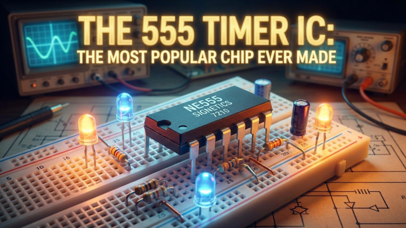
The 555 timer IC is a versatile integrated circuit used to generate precise timing signals, oscillations, and pulse waveforms. First introduced by Signetics in 1972, it remains the world’s best-selling IC with over one billion units produced annually — used in everything from hobby blinking LED circuits to industrial timing equipment and medical devices.
Introduction: The Chip That Refuses to Die
In the world of electronics, fashions change quickly. Components that dominated circuit design one decade are often obsolete the next, replaced by newer, smaller, more integrated alternatives. Microcontrollers have replaced entire boards of logic chips. Surface-mount devices have displaced through-hole components. Digital signal processors handle tasks once requiring dozens of analog circuits.
And yet, through five decades of relentless technological change, one humble integrated circuit has endured. The 555 timer IC — a chip designed in 1971 by Hans Camenzind for Signetics Corporation — remains in continuous production, active development, and widespread use today. Over a billion units are manufactured every year. It appears in toys, clocks, medical equipment, industrial controllers, musical instruments, and countless hobbyist projects worldwide.
Why has this chip survived? The answer lies in its elegant internal design, remarkable versatility, wide operating range, robustness, and extremely low cost. The 555 can function as a precise timer, a free-running oscillator, a pulse-width modulator, a frequency divider, a voltage-controlled oscillator, a touch sensor, a missing pulse detector, and more — all with just a handful of external resistors and capacitors.
For anyone learning electronics, the 555 timer is not just historically interesting — it’s a practically essential component to understand. The principles it demonstrates — RC timing circuits, comparators, flip-flops, and output drivers — are fundamental to electronics design. Understanding the 555 thoroughly gives you insight into timing circuits, oscillators, and control logic that applies far beyond this single chip.
This article provides a complete guide to the 555 timer: its history, internal architecture, pin-by-pin explanation, operating modes, design calculations, practical circuits, and tips for real-world use. By the end, you’ll have the knowledge to confidently use the 555 in your own projects and to understand why this remarkable chip has stood the test of time.
A Brief History: The Birth of the 555
In 1970, Hans Camenzind was a freelance circuit designer working for Signetics, a semiconductor company based in California. Signetics commissioned him to design a versatile timer IC that could compete with existing timing solutions, which typically required multiple chips and numerous external components.
Camenzind’s design brief was straightforward: create a timer circuit that was accurate, easy to use, robust, and manufacturable cheaply. He spent about a year on the design, working through multiple iterations before arriving at the architecture that became the 555.
The “555” designation comes from the three 5kΩ resistors that form the voltage divider at the heart of the chip’s internal reference circuit. Camenzind submitted the design in 1971. Signetics released it as the SE555/NE555 in 1972, and it was an immediate success.
Other manufacturers quickly produced licensed and unlicensed versions, driving down the price and establishing the 555 as an industry standard. Texas Instruments, STMicroelectronics, Fairchild, ON Semiconductor, and dozens of others have all manufactured 555-compatible chips. Today, a single NE555 in a DIP-8 package costs less than $0.50 in small quantities — less than a cup of coffee.
The chip’s longevity is a testament to the quality of the original design. In an era where integrated circuits have advanced from thousands to billions of transistors, the 555’s internal circuit contains just about 25 transistors, 2 diodes, and 15 resistors. Its simplicity is its strength.
The 555 Timer Family
Several versions of the 555 exist, each suited to slightly different applications:
| Part Number | Type | Description |
|---|---|---|
| NE555 / LM555 | Single timer | Standard commercial grade, 0°C to 70°C |
| SE555 | Single timer | Military/industrial grade, −55°C to 125°C |
| NE556 / LM556 | Dual timer | Two 555 circuits in a 14-pin DIP package |
| NE558 | Quad timer | Four 555 circuits in a 16-pin DIP package |
| LMC555 | CMOS 555 | Low-power CMOS version, operates from 1.5V to 15V |
| TLC555 | CMOS 555 | Low-power, rail-to-rail output, higher frequency capability |
| ICM7555 | CMOS 555 | Ultra-low power (microwatts), suitable for battery operation |
For most applications, the NE555 or LM555 (functionally identical) is the standard choice. When low power consumption is critical — in battery-powered devices, for example — the CMOS variants (LMC555, ICM7555) are preferred. The CMOS versions also operate at lower supply voltages and can run at higher frequencies than the bipolar NE555.
Inside the 555: Understanding the Internal Architecture
To use the 555 effectively, you need to understand what’s happening inside it. The internal circuit might seem complex at first glance, but it’s built from familiar building blocks: a resistor voltage divider, two comparators, a flip-flop, a discharge transistor, and an output driver.
The Voltage Divider: Setting the Reference
At the heart of the 555’s internal circuit are three resistors, each 5kΩ, connected in series between the supply voltage (VCC) and ground. This resistor chain creates two reference voltages:
- Upper threshold: 2/3 × VCC (at the junction between the top and middle resistors)
- Lower threshold: 1/3 × VCC (at the junction between the middle and bottom resistors)
If the supply voltage is 9V, the upper threshold is 6V and the lower threshold is 3V. If the supply voltage is 5V, the thresholds are 3.33V and 1.67V. The thresholds automatically scale with supply voltage, which is one reason the 555 operates correctly across a wide supply voltage range (4.5V to 15V for the NE555).
The Control Voltage pin (pin 5) connects to the 2/3 VCC point. By applying an external voltage here, you can override the 2/3 threshold and shift the switching points — a feature used in voltage-controlled oscillator applications.
Two Comparators: The Sensing Elements
The 555 contains two comparators — analog circuits that compare two voltages and produce a digital output indicating which is larger.
Comparator 1 (the threshold comparator) compares the voltage at pin 6 (THRESHOLD) to the 2/3 VCC reference. If the THRESHOLD pin voltage exceeds 2/3 VCC, comparator 1 outputs a logic high.
Comparator 2 (the trigger comparator) compares the voltage at pin 2 (TRIGGER) to the 1/3 VCC reference. If the TRIGGER pin voltage falls below 1/3 VCC, comparator 2 outputs a logic high.
These two comparators monitor external capacitor voltages and determine when to switch the internal state.
The SR Flip-Flop: The Memory Element
The outputs of the two comparators feed an SR (Set-Reset) flip-flop — a simple memory element with two stable states. The flip-flop remembers the circuit’s current state (timing or idle) and changes state only when commanded by the comparators.
- When the TRIGGER comparator fires (TRIGGER pin below 1/3 VCC), it sets the flip-flop, which turns ON the output (logic high).
- When the THRESHOLD comparator fires (THRESHOLD pin above 2/3 VCC), it resets the flip-flop, which turns OFF the output (logic low).
The flip-flop provides hysteresis — the circuit doesn’t switch back and forth at a single threshold voltage, but instead requires the voltage to reach the upper threshold to turn off and the lower threshold to turn on. This prevents rapid oscillation at the switching points.
The Discharge Transistor
An NPN transistor inside the 555 is controlled by the flip-flop’s output. When the flip-flop is in the reset state (output low), this transistor is turned on, connecting pin 7 (DISCHARGE) to ground. This discharges any capacitor connected between pin 7 and VCC.
When the flip-flop is in the set state (output high), the discharge transistor is off, and the capacitor can charge freely.
The interplay between capacitor charging, the comparators monitoring the capacitor voltage, and the discharge transistor discharging the capacitor is the mechanism behind all 555 timing operations.
The Output Driver
The flip-flop’s state drives an output stage that can both source current (supply current to a load) and sink current (accept current from a load). The NE555’s output can drive up to 200mA — enough to directly drive an LED, small relay, or transistor base without additional buffering. The output swings close to the supply rails: output high is approximately VCC − 1.7V, and output low is approximately 0.1V.
Pin-by-Pin Reference
The 555 timer comes in an 8-pin DIP package. Understanding each pin’s function is essential before building any circuit.
| Pin | Name | Function |
|---|---|---|
| 1 | GND | Ground (negative supply) |
| 2 | TRIGGER | Input: output goes high when pulled below 1/3 VCC |
| 3 | OUTPUT | Timer output, 0 or VCC (−1.7V), up to 200mA |
| 4 | RESET | Active-low reset; pull high to VCC if unused |
| 5 | CONTROL VOLTAGE | Access to internal 2/3 VCC reference; bypass to GND with 10nF cap if unused |
| 6 | THRESHOLD | Input: output goes low when pulled above 2/3 VCC |
| 7 | DISCHARGE | Open-collector transistor to GND; connects to RC network |
| 8 | VCC | Positive supply, 4.5V to 15V (NE555) |
Critical Pin Notes
Pin 4 (RESET): This is an active-low reset — it resets the output to low when pulled to ground. If you’re not using the reset function (most basic circuits don’t), you must connect pin 4 directly to VCC. Leaving it floating can cause unpredictable behavior because the pin may float to a voltage that partially enables the reset function.
Pin 5 (CONTROL VOLTAGE): Even when not using the control voltage function, it’s good practice to connect pin 5 to ground through a 10nF (0.01µF) ceramic capacitor. This filters any noise on the internal reference voltage and improves timing accuracy. Some circuits work without it, but it’s a professional habit worth developing.
Pin 7 (DISCHARGE): This is not a ground pin, though beginners sometimes confuse it with one. It’s the collector of an internal NPN transistor whose emitter connects to ground. When the discharge transistor is on, pin 7 connects to ground through the transistor’s saturation resistance (about 10Ω to 50Ω). The capacitor in your RC timing network connects between pin 7 and VCC (through a resistor) to be discharged at the right time.
The Three Operating Modes
The 555 timer has three primary operating modes: astable, monostable, and bistable. Each mode uses the same internal circuitry but with different external component configurations.
Mode 1: Monostable (One-Shot) Mode
In monostable mode, the 555 produces a single output pulse of defined duration each time it’s triggered. The circuit has one stable state (output low) and one unstable state (output high). When triggered, it enters the unstable state, stays there for a precisely timed interval, then automatically returns to the stable state.
How it works:
In the idle state, the output is low and the internal discharge transistor holds pin 7 (and the capacitor C1) at ground. When a negative-going pulse on pin 2 (TRIGGER) drops below 1/3 VCC, the flip-flop sets, the output goes high, and the discharge transistor turns off, allowing capacitor C1 to charge through resistor R1 toward VCC.
As C1 charges, the voltage at pin 6 (THRESHOLD) rises. When this voltage crosses 2/3 VCC, the threshold comparator fires, resetting the flip-flop. The output goes low, the discharge transistor turns on, and C1 quickly discharges through pin 7. The circuit is back to its stable state, ready for the next trigger.
Timing formula:
The pulse duration T depends only on R1 and C1:
T = 1.1 × R1 × C1Where T is in seconds, R1 is in ohms, and C1 is in farads.
Example calculation:
For a 1-second output pulse:
- Choose C1 = 10µF
- R1 = T / (1.1 × C1) = 1 / (1.1 × 10×10⁻⁶) = 90,909Ω ≈ 91kΩ (use 100kΩ for a slightly longer pulse)
Practical applications of monostable mode:
- Debouncing switches: A button press produces a clean, single pulse of defined length regardless of mechanical bounce
- Missing pulse detector: Normally triggered repeatedly by a signal; if the signal stops, the output changes state
- Touch sensor: Human body capacitance on pin 2 can trigger the circuit
- One-shot delay: Delay an action by a precise time after a trigger event
- Alarm hold: Keep a relay energized for a fixed period after a sensor triggers
Important monostable note: The trigger pulse must be shorter than the desired output pulse duration. If the trigger remains low for longer than T, the output will stay high until the trigger goes high, then time out normally. Also, re-triggering during an active timing cycle has no effect on the standard NE555 — the timing continues to its natural conclusion.
Mode 2: Astable (Free-Running Oscillator) Mode
In astable mode, the 555 oscillates continuously between high and low output states with no stable resting state. It generates a square-ish wave indefinitely, requiring only a power supply and two resistors and a capacitor.
How it works:
With the trigger pin (2) connected to the threshold pin (6), and a capacitor C1 connected between these pins and ground, the capacitor alternately charges and discharges between 1/3 VCC and 2/3 VCC.
- When C1 is below 1/3 VCC, the trigger comparator fires, setting the flip-flop (output high, discharge transistor off). C1 charges through R1 + R2 toward VCC.
- When C1 reaches 2/3 VCC, the threshold comparator fires, resetting the flip-flop (output low, discharge transistor on). C1 discharges through R2 toward ground (pin 7).
- When C1 falls back to 1/3 VCC, the cycle repeats.
The capacitor charges through both R1 and R2, but discharges only through R2 (because pin 7 connects between R1 and R2). This means the high time is always longer than the low time — the standard astable 555 cannot produce a 50% duty cycle with the basic circuit.
Timing formulas:
t_high = 0.693 × (R1 + R2) × C1
t_low  = 0.693 × R2 × C1
T      = t_high + t_low = 0.693 × (R1 + 2×R2) × C1
f      = 1 / T = 1.44 / ((R1 + 2×R2) × C1)
Duty cycle = (R1 + R2) / (R1 + 2×R2) × 100%Example calculation:
For a 1kHz oscillator with approximately 60% duty cycle:
- Choose C1 = 100nF
- Rearrange: R1 + 2×R2 = 1.44 / (f × C1) = 1.44 / (1000 × 100×10⁻⁹) = 14,400Ω
- Choose R2 = 5kΩ and R1 = 4.4kΩ (use 4.7kΩ)
- Verify: f = 1.44 / ((4700 + 10000) × 100×10⁻⁹) = 1.44 / 0.00147 ≈ 979Hz ≈ 1kHz ✓
Achieving 50% duty cycle in astable mode:
To produce a true 50% duty cycle, add a diode (1N4148) in parallel with R2, oriented so it bypasses R2 during charging. Now C1 charges through R1 only and discharges through R2 only. Set R1 = R2 for equal high and low times.
Alternatively, connect the output to an inverter or use the output and its complement for symmetric waveforms.
Practical applications of astable mode:
- LED blinker: A 1Hz astable circuit makes an LED blink once per second
- Tone generator: Audio frequencies (20Hz to 20kHz) drive a speaker or buzzer
- Clock source: Provides timing pulses for digital logic circuits
- PWM generation: Varies duty cycle by adjusting R1, R2, or controlling pin 5
- Frequency/period measurement: Using a known oscillator as a time reference
- Metronome: Audio clicks at a user-adjustable rate for music practice
Mode 3: Bistable (Schmitt Trigger) Mode
In bistable mode, the 555 acts as a simple flip-flop or Schmitt trigger. There are two stable states, and external signals control which state the output is in. The circuit has no timing components — it simply responds to the TRIGGER and THRESHOLD (or RESET) inputs.
How it works:
Connect pin 2 (TRIGGER) and pin 6 (THRESHOLD) to different control inputs. Pulling pin 2 below 1/3 VCC sets the output high; pulling pin 6 above 2/3 VCC resets the output low (or use pin 4/RESET instead of pin 6).
This mode essentially uses the 555 as a high-current output flip-flop or a Schmitt trigger for cleaning up noisy digital signals.
Practical applications of bistable mode:
- Switch debouncer: Connect an SPDT switch to TRIGGER and RESET; output changes cleanly without bounce
- Schmitt trigger: Apply a slow-moving or noisy signal; output transitions cleanly at defined thresholds
- High-current buffer: The 200mA output capability makes the 555 bistable useful as a relay driver or motor controller
- Memory element: Retains state after the control signal is removed
Practical Circuit Examples
Project 1: LED Blinker (Astable, 1Hz)
Components:
- NE555 or LM555 IC
- R1 = 68kΩ
- R2 = 68kΩ
- C1 = 10µF electrolytic (observe polarity — negative to ground)
- C2 = 10nF ceramic (pin 5 bypass)
- LED + 470Ω current-limiting resistor
- 9V battery or regulated 9V supply
Circuit connections:
- Pin 1 → GND
- Pin 2 → Pin 6 (connected together)
- Pin 3 → 470Ω resistor → LED → GND
- Pin 4 → VCC (9V)
- Pin 5 → 10nF capacitor → GND
- Pin 6 → Positive terminal of C1 → GND (negative terminal)
- Pin 7 → Junction of R1 and R2
- R1 connects from VCC to pin 7
- R2 connects from pin 7 to pin 6
- Pin 8 → VCC (9V)
Calculated frequency: f = 1.44 / ((68k + 2×68k) × 10µF) = 1.44 / (204,000 × 10×10⁻⁶) = 1.44 / 2.04 ≈ 0.71Hz
The LED will blink approximately once every 1.4 seconds. To get closer to 1Hz, reduce R1 or R2 slightly, or use a smaller capacitor.
Project 2: Doorbell Tone Generator (Astable, Audio)
Components:
- NE555
- R1 = 1kΩ
- R2 = 10kΩ (variable potentiometer for adjustable pitch)
- C1 = 47nF
- C2 = 10nF (pin 5 bypass)
- Small 8Ω speaker with 100µF coupling capacitor in series
Calculated frequency range: With R2 at minimum (0Ω): f = 1.44 / ((1k + 0) × 47nF) = 30.6kHz (ultrasonic, silent) With R2 at maximum (10kΩ): f = 1.44 / ((1k + 20k) × 47nF) = 1.46kHz (pleasant tone)
Adjust R2 to change pitch. This simple circuit produces a pleasant tone suitable for alarms, toys, and audio alerts.
Project 3: Timed Relay (Monostable)
Components:
- NE555
- R1 = 470kΩ
- C1 = 100µF electrolytic
- C2 = 10nF (pin 5 bypass)
- Momentary push button (normally high via 10kΩ pull-up, pressed to GND)
- Small 5V relay module (coil driven from pin 3 output)
- 1N4007 flyback diode across relay coil
Calculated pulse duration: T = 1.1 × 470,000 × 100×10⁻⁶ = 1.1 × 47 = 51.7 seconds
Press the button, and the relay energizes for approximately 52 seconds, then releases. Adjust R1 or C1 to change the timing. This circuit is the basis for stairwell lighting timers, door-lock delays, and automatic shut-off circuits.
Design Guidelines and Common Mistakes
Resistor and Capacitor Selection
For timing resistors, use values between 1kΩ and 10MΩ. Below 1kΩ, the output stage may not be able to maintain stable output voltages while also charging the capacitor. Above 10MΩ, leakage currents in the capacitor and circuit board become significant compared to the timing current, degrading accuracy.
For timing capacitors, electrolytic capacitors work for long time periods (above about 100ms) but have high leakage and tolerance (±20% or worse), limiting timing accuracy. For precise, short timing intervals, use polyester film, polypropylene, or ceramic capacitors with tighter tolerances (±5% or ±1%).
Never use very large electrolytic capacitors (above about 100µF) in timing circuits without accounting for their leakage current. A 1000µF capacitor with 1µA leakage will cause significant error with high-value timing resistors.
Power Supply Decoupling
The 555’s output stage switches 200mA abruptly, causing voltage spikes on the supply rail that can affect other circuits and even destabilize the 555’s own timing. Always place a 100nF ceramic capacitor between VCC and GND as close to pin 8 as possible, plus a 10µF electrolytic nearby for bulk decoupling.
The RESET Pin: Never Leave It Floating
Pin 4 (RESET) must be connected to VCC if not used. A floating reset pin is one of the most common causes of erratic 555 behavior — especially if there’s electrical noise in the environment or other circuitry nearby. The reset function is active-low with a threshold of about 0.7V. Noise can easily pull a floating pin to this level and randomly reset the timer.
Output Loading
The NE555 can source or sink up to 200mA — a genuinely useful output drive capability. However, this doesn’t mean you should drive loads right at the limit. At maximum current, the output voltage drops significantly from VCC. For an LED, a current-limiting resistor is still essential. For relay coils and motors, a flyback diode across the inductive load is mandatory to suppress the voltage spike when current is interrupted.
Timing Accuracy and Temperature
The NE555’s timing depends on the threshold voltages being exactly 1/3 and 2/3 VCC, which requires the three internal 5kΩ resistors to be well-matched. In practice, timing accuracy is typically ±1% at room temperature. Temperature coefficient of the NE555 is about 50ppm/°C — meaning the timing period changes by 0.005% per degree Celsius. For precision timing applications, the CMOS variants (LMC555, ICM7555) offer better temperature stability, and the external RC components should use precision resistors and stable capacitors.
Maximum Operating Frequency
The standard bipolar NE555 operates reliably up to about 300kHz in astable mode. Above this frequency, the output waveform degrades as the internal propagation delays become significant relative to the timing period. CMOS variants like the TLC555 operate at higher frequencies, up to several megahertz.
Advanced 555 Applications
Beyond basic timing and oscillation, the 555’s versatility enables sophisticated applications that demonstrate the chip’s depth.
Voltage-Controlled Oscillator (VCO)
By applying a control voltage to pin 5 (CONTROL VOLTAGE), the internal reference thresholds shift, changing the timing period and thus the output frequency. As the control voltage increases, the thresholds increase, the capacitor takes longer to charge and discharge, and the frequency decreases. This creates a linear relationship between control voltage and frequency — a voltage-controlled oscillator.
VCO applications include: electronic music synthesizers (voltage controls pitch), frequency modulation circuits, and motor speed feedback loops.
PWM Generator
In astable mode with a control voltage applied to pin 5, the duty cycle changes while the frequency remains approximately constant. This creates a simple pulse-width modulator useful for LED dimming, motor speed control, and audio generation.
Connect a potentiometer between VCC and GND, with the wiper going to pin 5. Rotating the pot changes the PWM duty cycle from near 0% to near 100%, providing smooth analog control of a digital output.
Frequency Divider
By connecting the output of one 555 in astable mode to the trigger input of another 555 in monostable mode, you can create frequency dividers. Each trigger pulse generates one output pulse, and by carefully sizing the monostable’s timing components, you can ensure it only responds to every Nth trigger pulse — effectively dividing the frequency.
Missing Pulse Detector
Connect an input signal to pin 2 (TRIGGER) of a monostable 555 with a timing period slightly longer than the expected pulse interval. Under normal operation, each incoming pulse re-triggers the monostable before it times out, keeping the output continuously high. If a pulse is missed, the monostable times out and the output goes low — signaling that the input pulse stream has stopped or slowed. This circuit monitors heartbeats, machine cycles, or encoder pulses and alerts when they stop.
Touch Sensor
The TRIGGER pin has a threshold of 1/3 VCC — for a 9V supply, that’s 3V. Human body capacitance and resistance can pull pin 2 low when touched, triggering the monostable output. A simple touch pad connected to pin 2 through a 1MΩ resistor creates a touch-activated timer. The high input impedance of pin 2 makes this possible with no external power source needed to the touch pad.
The 555 in Context: Why It Still Matters
In an age of $2 microcontrollers that can perform thousands of timing functions in software, why does the 555 still matter? Several reasons:
No programming required: The 555 works immediately with the right RC values. There’s no compiler, no IDE, no firmware to write or debug. For simple timing tasks, the 555 is faster to implement than any programmable solution.
Robustness and reliability: The 555 operates from 4.5V to 15V without adjustment. It tolerates supply voltage variations gracefully — timing accuracy doesn’t depend on a precise reference voltage. It works in extreme temperatures, survives input voltage transients that would damage microcontrollers, and requires no initialization sequence.
Output drive capability: The 555’s 200mA output can directly drive relays, motors, and other loads that require additional transistor stages with a microcontroller. This reduces component count in high-current applications.
Teaching value: The 555 beautifully illustrates fundamental electronics concepts: voltage dividers, comparators, flip-flops, RC timing, and output drivers. Understanding the 555 deeply provides insight into circuits that is more educational than calling a software timer function.
Analog integration with digital output: The 555 bridges analog and digital domains naturally. Its thresholds track the supply voltage, and its timing responds to external voltages applied to pin 5 — behaviors that are difficult to replicate purely in software.
The 555 is not always the best choice for modern designs. When timing precision below ±0.1% is needed, crystal-controlled oscillators or real-time clock ICs are better. When complex timing sequences are needed, microcontrollers are more appropriate. When ultra-low power is essential, dedicated timer ICs with nanoamp quiescent currents outperform even the CMOS 555.
But for a vast range of practical timing applications — especially in prototyping, education, and low-cost production — the 555 remains a fast, cheap, reliable solution that has earned its place in electronics history.
Quick Reference: Essential 555 Formulas
| Mode | Formula | Variables |
|---|---|---|
| Monostable pulse width | T = 1.1 × R1 × C1 | T in seconds, R in ohms, C in farads |
| Astable high time | t_H = 0.693 × (R1 + R2) × C1 | — |
| Astable low time | t_L = 0.693 × R2 × C1 | — |
| Astable frequency | f = 1.44 / ((R1 + 2R2) × C1) | f in Hz |
| Astable duty cycle | D = (R1 + R2) / (R1 + 2R2) | D as decimal |
Summary
The 555 timer IC is a masterpiece of analog design that has endured for over 50 years because it solves real problems elegantly and inexpensively. Its internal architecture — three resistors forming reference voltages, two comparators monitoring a capacitor, a flip-flop remembering state, a discharge transistor resetting the timing, and a high-current output driver — provides a versatile platform for timing, oscillation, and pulse generation.
In monostable mode, it generates a single timed pulse of controllable duration. In astable mode, it oscillates freely to produce square waves for clocks, audio tones, and PWM signals. In bistable mode, it acts as a robust flip-flop or Schmitt trigger. With external components totaling a resistor, another resistor, and a capacitor, it covers timing ranges from microseconds to hours.
The 555 teaches core electronics principles while remaining a practical, production-worthy component. Whether you’re blinking an LED, controlling a relay, generating an audio tone, or exploring analog circuit design, the 555 timer is a tool worth mastering.