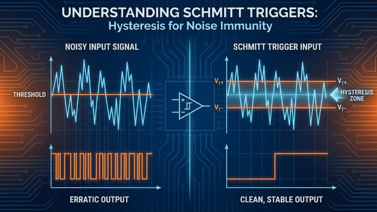
A Schmitt trigger is a comparator circuit with built-in hysteresis — two separate switching thresholds that create a dead band preventing false triggering from noise. The output switches to a high state only when the input rises above the upper threshold and returns to a low state only when the input falls below the lower threshold, making Schmitt triggers essential for converting noisy analog signals into clean digital transitions in switches, sensors, oscillators, and logic interfaces.
Introduction: The Circuit That Refuses to Be Fooled by Noise
In an ideal world, digital signals would have perfectly sharp transitions, analog signals would be perfectly clean, and every circuit would behave exactly as designed. In the real world, none of these things are true.
Digital signals in real systems have edges that take nanoseconds to transition, and during those edges they pass through the undefined region between logic HIGH and logic LOW. Analog signals carry noise from thermal agitation, electromagnetic pickup, power supply coupling, and ground bounce. Long cable runs pick up interference from motors, switching supplies, and radio transmitters. Mechanical switches bounce dozens of times before settling. Capacitively coupled signals from adjacent wires can appear as phantom voltage variations on signal lines.
All of these imperfections create a common problem: a signal that should cleanly cross a threshold once instead crosses it multiple times, triggering multiple responses where only one was intended. A button press registers as ten. A temperature threshold triggers an alarm that turns on and off dozens of times per second. A logic signal that should transition cleanly oscillates back and forth, corrupting downstream circuit operation.
The Schmitt trigger is the standard engineering solution to all of these problems. Named after American scientist Otto Schmitt who described the circuit in 1934, the Schmitt trigger adds a single powerful property to a comparator: memory of its own output state. The threshold at which the circuit switches depends on which state the output is currently in. To switch from LOW to HIGH, the input must rise above the upper threshold. To switch from HIGH to LOW, the input must fall below the lower threshold — a lower voltage. Between these two thresholds is the hysteresis band: a dead zone where input changes produce no output change.
This hysteresis band is what eliminates noise sensitivity. As long as noise amplitude is smaller than the hysteresis band, noise cannot cause false switching. The output changes state only in response to definitive, meaningful input transitions — not fleeting noise excursions.
The Schmitt trigger is not a single specific circuit but a general principle — hysteresis applied to a comparator. It can be implemented with op-amps using positive feedback, with dedicated Schmitt trigger ICs (74HC14, 74HC132, SN74LS13), or as an inherent property of certain integrated circuits designed for noisy environments. Every digital oscilloscope input has a Schmitt trigger. Every microcontroller’s external interrupt pin has a Schmitt trigger. Every button or switch interface in professional electronics uses Schmitt trigger conditioning.
This article provides a complete, deeply practical guide to Schmitt triggers: the physics of hysteresis, mathematical derivations of threshold voltages for all standard configurations, dedicated Schmitt trigger IC specifications and applications, oscillator designs based on Schmitt triggers, and a comprehensive set of practical circuits covering switch debouncing, long-cable signal conditioning, clock signal generation, and noise-immune sensor interfaces.
The Physics of Hysteresis: Why Two Thresholds Beat One
The Single-Threshold Problem Revisited
Consider a comparator with a single threshold at exactly 2.5V. The input signal is nominally 2V (LOW) or 3V (HIGH), but carries 300mV peak-to-peak noise. As the signal transitions from 2V to 3V, passing through 2.5V:
- At 2.2V: input still below threshold, output LOW — correct
- At 2.4V: input below threshold, output LOW — correct
- At 2.5V: crosses threshold — output goes HIGH
- Noise spike pulls signal back to 2.3V: crosses threshold downward — output goes LOW again
- Signal continues rising, hits 2.5V again — output goes HIGH again
- Another noise excursion pulls it to 2.4V — output LOW again
The result is a burst of multiple output transitions during what should be a single clean switching event. Depending on noise amplitude and transition speed, there could be 5, 10, or 50 output pulses during one intended transition.
The Two-Threshold Solution
Now imagine the comparator has two thresholds: V_TH+ = 2.8V (upper, for switching HIGH) and V_TH− = 2.2V (lower, for switching LOW). The hysteresis band is 0.6V — twice the noise amplitude.
The signal starts at 2V (LOW), output is LOW. As the signal rises with 300mV noise:
- At 2.5V: peak noise might reach 2.65V — still below 2.8V, output stays LOW
- At 2.7V: peak noise might reach 2.85V — might just cross 2.8V, but only briefly
- At 2.9V: signal clearly above 2.8V even accounting for noise — output switches HIGH (once, cleanly)
Once the output is HIGH, to switch back LOW the input must fall below 2.2V. Even with 300mV noise at 2.5V (nominal HIGH level), the lowest the signal goes is 2.2V — right at the lower threshold. At 2.4V nominal HIGH level, the signal is safely above 2.2V and stays HIGH.
The hysteresis band has absorbed the noise. The output changes state only when the input makes a definitive, large-amplitude transition — not from noise fluctuations. This is the fundamental value of the Schmitt trigger.
The Hysteresis Loop
The Schmitt trigger’s input-output relationship draws as a rectangle on a graph of V_out vs. V_in — the hysteresis loop:
- As V_in increases from left: output stays LOW until V_in reaches V_TH+ (upper threshold), then snaps HIGH
- As V_in decreases from right: output stays HIGH until V_in falls to V_TH− (lower threshold), then snaps LOW
- The output traces a rectangular loop — traveling clockwise as input increases and counterclockwise as input decreases
The width of this rectangle is V_hys = V_TH+ − V_TH−. A wider rectangle means more noise immunity but requires a larger signal swing to trigger switching. A narrower rectangle is more sensitive but less immune to noise. Setting the right hysteresis band for the application is the central Schmitt trigger design decision.
Rule of Thumb for Hysteresis Band Sizing
V_hys = 3 × V_noise_peak_to_peak (minimum)
V_hys = 5 × V_noise_peak_to_peak (recommended for reliable operation)For a signal with 100mV peak-to-peak noise: V_hys = 300mV to 500mV. For a signal with 1V peak-to-peak noise: V_hys = 3V to 5V. For a mechanical switch with contact bounce: V_hys can be very large (the signal swings from 0V to VCC regardless of bounce), so any moderate hysteresis band works.
Schmitt Trigger Implementations
The Schmitt trigger principle can be implemented in three main ways: using an op-amp with positive feedback, using a dedicated comparator IC with positive feedback, or using dedicated Schmitt trigger logic ICs. Each approach suits different applications.
Implementation 1: Op-Amp Schmitt Trigger (Non-Inverting)
The non-inverting Schmitt trigger connects the input signal to V+ (through a resistor R1) and feeds back a fraction of the output to the same V+ node through R2. V− connects to the threshold reference voltage V_ref.
Circuit elements:
- V_in → R1 → V+ (non-inverting input)
- V_out → R2 → V+ (positive feedback)
- V_ref → V− (inverting input, sets center threshold)
The voltage at V+ is a weighted average of V_in and V_out:
V+ = V_in × (R2 / (R1 + R2)) + V_out × (R1 / (R1 + R2))The comparator switches when V+ = V_ref = V−.
Solving for the thresholds:
When output is LOW (V_OL):
V+ = V_in × R2/(R1+R2) + V_OL × R1/(R1+R2) = V_ref
V_TH+ = (V_ref × (R1+R2) − V_OL × R1) / R2
V_TH+ = V_ref × (1 + R1/R2) − V_OL × (R1/R2)When output is HIGH (V_OH):
V_TH− = V_ref × (1 + R1/R2) − V_OH × (R1/R2)Hysteresis voltage:
V_hys = V_TH+ − V_TH− = (V_OH − V_OL) × R1/R2The hysteresis is proportional to the output swing (V_OH − V_OL) and the ratio R1/R2. To increase hysteresis: increase R1, decrease R2, or both.
Worked example: VCC = ±12V supply, V_ref = 0V (threshold centered on 0V), V_OH = +11V, V_OL = −11V, desired hysteresis = 1V:
V_hys = (V_OH − V_OL) × R1/R2
1V = (11 − (−11)) × R1/R2 = 22 × R1/R2
R1/R2 = 1/22 → use R1 = 4.7kΩ, R2 = 100kΩ (ratio ≈ 1/21.3, V_hys ≈ 1.03V)With V_ref = 0V:
V_TH+ = 0 × (1 + 4.7/100) − (−11) × (4.7/100) = 0 + 11 × 0.047 = +0.517V
V_TH− = 0 × (1 + 0.047) − 11 × 0.047 = −0.517VSymmetric thresholds at ±0.517V — the circuit switches HIGH when input exceeds +517mV and switches LOW when input falls below −517mV.
Implementation 2: Op-Amp Schmitt Trigger (Inverting)
The inverting Schmitt trigger places the input signal at V− and the positive feedback at V+. The behavior is inverted: output goes LOW when input rises above threshold, HIGH when it falls below.
Circuit elements:
- V_in → V− (inverting input directly)
- R1 from VCC to V+
- R2 from V+ to ground
- R3 from output to V+ (positive feedback)
The voltage at V+ depends on the current output state and the resistor network. When the output is HIGH (V_OH), the positive feedback raises V+, increasing the threshold. When LOW (V_OL), it lowers V+.
Threshold equations (simplified for V_OL = 0V, R_gnd in parallel with R_feedback):
For the common configuration with reference divider R1, R2 and feedback R_f:
V_TH+ = V_OH × R2 / (R1 + R2)   [threshold when output is HIGH → transition to LOW]
V_TH− = V_OL × R2 / (R1 + R2) [threshold when output is LOW → transition to HIGH]With V_OL = 0V: V_TH− = 0 × anything = 0V (lower threshold is at ground) With V_OH = 5V: V_TH+ = 5V × R2/(R1+R2)
For R1 = 10kΩ, R2 = 10kΩ: V_TH+ = 2.5V, V_TH− = 0V, V_hys = 2.5V
This large asymmetric hysteresis is characteristic of the simple inverting Schmitt with a grounded lower resistor — useful when the signal swings from ground to VCC (digital signals, switch contacts).
General inverting Schmitt trigger design:
For symmetrical thresholds centered on V_center with hysteresis V_hys:
V_center = (V_TH+ + V_TH−) / 2
V_TH+ = V_center + V_hys/2
V_TH− = V_center − V_hys/2Set the base threshold with a voltage divider on V+, then calculate the positive feedback resistor to achieve the desired hysteresis spread.
Implementation 3: Dedicated Schmitt Trigger Logic ICs
For digital signal conditioning in logic circuits, dedicated Schmitt trigger ICs are the most efficient solution. These integrate the comparator with hysteresis directly into a logic gate package — no external resistors needed.
74HC14 — Hex Inverting Schmitt Trigger
The 74HC14 contains six independent inverting Schmitt trigger buffers in a 14-pin DIP or SOIC package. Each input has built-in hysteresis:
- VCC = 5V: V_TH+ ≈ 2.4V, V_TH− ≈ 1.6V, V_hys ≈ 0.8V (minimum 0.5V guaranteed)
- VCC = 3.3V: V_TH+ ≈ 1.6V, V_TH− ≈ 0.9V, V_hys ≈ 0.7V (approximately)
The output inverts the input: a rising input above V_TH+ produces a LOW output; a falling input below V_TH− produces a HIGH output.
74HC132 — Quad 2-Input NAND with Schmitt Trigger Inputs
Four 2-input NAND gates with Schmitt trigger inputs. Both inputs have hysteresis, making the gate immune to noise on either input. Useful for cleaning up two noisy signals before logical combination.
74HC7414 / SN74LS14 — Also hex inverting Schmitt triggers, but in LS TTL logic family (lower speed, higher power than HC).
CD40106 — CMOS Hex Inverting Schmitt Trigger
The CMOS variant, operating from 3V to 18V supply. Hysteresis is approximately 30–40% of VCC — much wider than the HC family. At 5V: V_hys ≈ 1.5–2.0V. At 12V: V_hys ≈ 3.6–4.8V. This very wide hysteresis makes the CD40106 excellent for oscillator circuits and for conditioning very noisy signals.
Key advantages of dedicated Schmitt trigger ICs:
- No external resistor calculation needed
- Guaranteed minimum hysteresis (specified in datasheet)
- Fast transition speed (typically 5–15ns output rise/fall time for 74HC family)
- Low power consumption
- Directly outputs standard logic levels
- Six gates per package — cost-effective for multiple signals
Limitation: Fixed hysteresis band determined by the IC design and supply voltage. If the noise exceeds the built-in hysteresis, additional filtering or a higher hysteresis external circuit is needed.
Schmitt Trigger Oscillators
One of the most elegant applications of the Schmitt trigger is as an oscillator. By combining a Schmitt trigger with an RC network, you create a self-sustaining oscillator that needs no quartz crystal, no tuned LC circuit, and no complex timing components — just two resistors and a capacitor.
The RC Schmitt Trigger Oscillator
Circuit using 74HC14 or CD40106:
Connect a resistor R from the output back to the input. Connect capacitor C from the input to ground. This is the complete oscillator — three components (one Schmitt trigger, one resistor, one capacitor).
How it oscillates:
- Assume the output is HIGH (5V). The capacitor begins charging toward 5V through R.
- When the capacitor voltage reaches V_TH+ (the upper threshold, ~2.4V for 74HC14), the Schmitt trigger output switches LOW (0V).
- Now the capacitor begins discharging toward 0V through R.
- When the capacitor voltage falls to V_TH− (the lower threshold, ~1.6V for 74HC14), the Schmitt trigger output switches HIGH (5V) again.
- Repeat indefinitely.
The capacitor alternately charges from V_TH− to V_TH+ (when output is HIGH) and discharges from V_TH+ to V_TH− (when output is LOW).
Frequency calculation:
The charging time (output HIGH):
t_high = R × C × ln((V_OH − V_TH−) / (V_OH − V_TH+))The discharging time (output LOW):
t_low = R × C × ln(V_TH+ / V_TH−)For a 74HC14 with VCC = 5V (V_OH = 5V, V_TH+ = 2.4V, V_TH− = 1.6V):
t_high = RC × ln((5 − 1.6) / (5 − 2.4)) = RC × ln(3.4/2.6) = RC × ln(1.308) = RC × 0.268
t_low  = RC × ln(2.4/1.6) = RC × ln(1.5) = RC × 0.405
T = RC × (0.268 + 0.405) = RC × 0.673
f = 1/T ≈ 1.49 / (R × C)Note: The exact frequency depends on the specific 74HC14’s threshold voltages, which vary between manufacturers and batches (the datasheet only guarantees minimum hysteresis). For reliable frequency-setting, the CD40106’s wider hysteresis provides more predictable behavior, or use the 555 timer (whose thresholds are set by an accurate internal voltage divider).
Practical oscillator design example:
Target: 10kHz oscillator, VCC = 5V, using 74HC14:
f ≈ 1.49 / (R × C)
R × C = 1.49 / 10,000 = 149µsChoose C = 10nF: R = 149µs / 10nF = 14.9kΩ → use 15kΩ (E24 series)
Verify: f = 1.49 / (15,000 × 10×10⁻⁹) = 1.49 / 150µs = 9.93kHz ≈ 10kHz ✓
Target: 1Hz oscillator (for a slow blinking LED):
R × C = 1.49 / 1 = 1.49sChoose C = 10µF: R = 1.49s / 10µF = 149kΩ → use 150kΩ
Frequency range: Using the 74HC14, practical oscillation range is from sub-Hz (with large RC) to approximately 10–20MHz (with small RC, limited by gate propagation delay). Above about 1MHz, the RC oscillator’s frequency becomes significantly affected by the gate’s propagation delay — use a crystal oscillator for high-frequency precision.
Oscillator Frequency Stability
The RC Schmitt trigger oscillator’s frequency depends on:
- R and C values (main determinants)
- The Schmitt trigger’s threshold voltages (which vary between ICs and with temperature)
- Supply voltage (threshold voltages scale with VCC for some CMOS types)
- Temperature (R and C both have temperature coefficients)
Typical frequency accuracy: ±10–30% without calibration, ±5% with component selection.
For better stability: use a resistor with low temperature coefficient (metal film, 50–100ppm/°C) and a C0G/NP0 ceramic capacitor or film capacitor (±30–50ppm/°C). This limits temperature-induced frequency drift to approximately 0.01–0.03% per °C — adequate for most non-precision timing applications.
For precision timing, replace the RC oscillator with a crystal-controlled clock and use the Schmitt trigger only for signal conditioning.
Schmitt Trigger Applications
Application 1: Mechanical Switch Debouncing
Mechanical switches bounce — the contacts make and break contact dozens of times in the first millisecond after actuation before settling. A digital circuit sees this as multiple rapid transitions rather than a single clean edge.
Why the Schmitt trigger helps: Connect the switch between VCC and the Schmitt trigger input, with a pull-down resistor (10kΩ) to ground. A small capacitor (100nF) from the input to ground integrates the bouncing signal:
- When the switch closes: VCC charges through the closed switch and 100nF capacitor. Multiple bounce-induced disconnections cause the capacitor to partially discharge each time. But the capacitor slows the voltage changes — instead of sharp transitions, the input voltage rises and falls gradually.
- The RC time constant is R_switch_closed (very low, maybe 100Ω) × 100nF ≈ 10µs for charging, and 10kΩ × 100nF = 1ms for discharging.
- Bounce duration: typically 1–10ms.
During bounce, the capacitor voltage fluctuates but only changes by a limited amount per bounce event. The Schmitt trigger’s hysteresis band absorbs these fluctuations — the output doesn’t switch unless the capacitor voltage definitively passes the appropriate threshold.
Full debounce circuit:
- Switch from VCC to node A (with 100Ω series resistor to limit current)
- R_pull = 10kΩ from node A to GND (ensures defined state when switch open)
- C_debounce = 100nF from node A to GND (integrates bounce)
- 74HC14 Schmitt trigger with input at node A
Timing: The RC time constant is 10kΩ × 100nF = 1ms. This is the time for the input to transition through the hysteresis band after a switch event. Bounce events shorter than ~1ms are absorbed. Press and release detection are each debounced cleanly.
For switch bounce that exceeds 10ms (old or worn switches), increase C_debounce to 1µF (10ms time constant) or 10µF (100ms).
Application 2: Long-Cable Signal Conditioning
Long cables pick up noise from multiple sources: nearby power cables inducing voltage through mutual inductance, radio frequency interference, capacitive coupling from adjacent signals, and ground potential differences between the transmitting and receiving ends.
A digital signal traveling 10 meters of unshielded cable might arrive with 500mV to 2V of superimposed noise — enough to cause multiple false transitions at a standard digital input.
Schmitt trigger solution: At the receiving end, connect the cable to a Schmitt trigger input (74HC14 or comparator with hysteresis) rather than a standard digital gate.
Enhanced approach for very noisy environments:
- Terminate the cable at its characteristic impedance (120Ω for twisted pair)
- Add a small RC filter (100Ω + 1nF) before the Schmitt trigger input to attenuate high-frequency noise above the signal bandwidth
- Use the Schmitt trigger to restore clean logic levels from the filtered, but potentially still noise-contaminated, signal
For RS-485 differential signals: The differential receiver already rejects common-mode noise, but a Schmitt trigger on the output further improves immunity to residual differential noise near the decision threshold.
Application 3: Sine Wave to Square Wave Converter
Many signal sources produce sine waves — oscillators, transformers, function generators, audio sources. Digital circuits need square waves. A Schmitt trigger performs the conversion cleanly.
Simple conversion: Connect the sine wave directly to a Schmitt trigger input. As the sine wave rises through V_TH+, the output switches (LOW for inverting Schmitt). As it falls through V_TH−, the output switches back.
Result: A square wave at the same frequency as the sine wave, with sharp digital edges. The Schmitt trigger’s hysteresis prevents noise near the zero crossing from causing multiple transitions per cycle.
Centering the threshold: For a sine wave centered on 0V (typical oscillator output), use a Schmitt trigger with thresholds centered on 0V — which requires a dual-supply Schmitt trigger or an op-amp Schmitt trigger with V_ref = 0V.
For a single-supply circuit receiving an AC-coupled sine wave: the sine wave must be DC-biased to mid-supply (VCC/2) before reaching the Schmitt trigger input. Use a coupling capacitor and pull-up/pull-down resistor network to set the DC level.
Worked example: Convert a 10kHz, 5V peak-to-peak sine wave (centered on 0V) to a TTL square wave using a ±5V op-amp Schmitt trigger:
Op-amp (TL071), V_ref = 0V at V−, R1 = 10kΩ, R2 = 100kΩ feedback:
V_hys = (V_OH − V_OL) × R1/R2 = (5 − (−5)) × 10k/100k = 10 × 0.1 = 1V
V_TH+ = +0.5V, V_TH− = −0.5VThe sine wave easily exceeds ±0.5V, ensuring clean switching. Any noise below 0.5V amplitude is rejected.
Application 4: Touch Sensor Interface with Noise Immunity
Resistive touch sensors have high output impedance and are susceptible to capacitive coupling interference. A Schmitt trigger provides clean output from a noisy, slow-changing touch signal.
Circuit:
- Touch pad (bare copper area) connected to input through 1MΩ resistor
- 10pF capacitor from input to ground (filters high-frequency RF interference)
- 10MΩ pull-up resistor from input to VCC (defines untoched state)
- Schmitt trigger (74HC14) with input connected to the touch pad node
When untouched: input pulled to VCC through 10MΩ → output LOW (inverting Schmitt) When touched: human body resistance (~1MΩ) in parallel with 10MΩ pull-up pulls input down → output HIGH
The Schmitt trigger’s hysteresis prevents the noisy, capacitively-coupled environment near the touch pad from causing false triggering.
Application 5: Brownout / Power-Good Detection
Goal: Generate a clean POWER_GOOD signal when supply voltage is above 4.5V and POWER_FAIL when below 4.2V (0.3V hysteresis band).
Circuit:
- VCC (5V nominal) → voltage divider → comparator non-inverting input
- Stable 2.5V reference → comparator inverting input
- Positive feedback resistor for hysteresis
- Output: POWER_GOOD logic signal
Threshold setup: Want comparator to switch HIGH when VCC > 4.5V: Divide VCC by 2 using a voltage divider (R1 = R2 = 100kΩ): V_div = VCC/2
When VCC = 4.5V: V_div = 2.25V — set V_ref slightly below this. Use V_ref = 2.2V, add hysteresis of 150mV (so lower threshold corresponds to VCC = 4.2V):
Lower threshold: V_div_low = V_ref − V_hys/2 = 2.2V − 0.075V = 2.125V → VCC = 4.25V ≈ 4.2V ✓ Upper threshold: V_div_high = V_ref + V_hys/2 = 2.2V + 0.075V = 2.275V → VCC = 4.55V ≈ 4.5V ✓
Hysteresis resistor calculation: With R1 = R2 = 100kΩ (voltage divider), V_ref = 2.2V, V_hys = 150mV, V_OH = 3.3V, V_OL = 0V:
R_feedback = R_divider_parallel × (V_OH − V_OL) / V_hys
R_divider_parallel = 100k ∥ 100k = 50kΩ
R_feedback = 50,000 × (3.3 − 0) / 0.15 = 50,000 × 22 = 1.1MΩ → use 1MΩThe POWER_GOOD signal is HIGH only when the supply is definitively above 4.5V, with no ambiguous switching as voltage slowly rises through 4.3V.
Schmitt Trigger in Digital Logic: Input Hysteresis
Modern digital logic families include Schmitt trigger inputs on specific pin types precisely because real-world signal edges are never instantaneous.
Why Digital Logic Needs Schmitt Triggers
A standard digital gate (74HC00 NAND gate, for example) has very narrow defined logic thresholds — V_IH minimum (the lowest voltage guaranteed to be read as HIGH) and V_IL maximum (the highest voltage guaranteed to be read as LOW). Between these thresholds is the undefined region where the output is unpredictable.
A signal transitioning through this undefined region should do so as quickly as possible. But many real-world signals are slow:
- RC-filtered clock signals with gentle slopes
- Long cable signals with capacitance-limited rise times
- Crystal oscillator outputs during startup (amplitude is small)
- Reset signals generated by RC circuits
When a slowly transitioning signal passes through the undefined region of a standard logic gate, the gate may oscillate, outputting multiple pulses. A Schmitt trigger input solves this by making the switching decision definitive — once the input crosses V_TH+, the output snaps LOW (for inverting), and it won’t switch back until the input falls below V_TH− — well outside the undefined region.
Schmitt Trigger Specifications in Microcontrollers
Most modern microcontrollers have Schmitt trigger inputs on at least some pins. Checking the ATmega328P (used in Arduino Uno) datasheet:
- All I/O pins have Schmitt trigger inputs by default
- V_TH+ (input high threshold) ≈ 0.7 × VCC = 3.5V at VCC = 5V
- V_TH− (input low threshold) ≈ 0.3 × VCC = 1.5V at VCC = 5V
- V_hys = V_TH+ − V_TH− = 2.0V (40% of VCC)
This 2V hysteresis band means a signal must be clearly above 3.5V to register as HIGH and clearly below 1.5V to register as LOW — noise of up to 1V in amplitude cannot cause false switching between these states.
For the STM32 family ARM microcontrollers, Schmitt trigger thresholds are approximately:
- VDD = 3.3V: V_TH+ ≈ 1.5V, V_TH− ≈ 0.5V (approximate, varies by product)
External Schmitt Trigger Conditioning for Microcontroller Inputs
When connecting external signals to microcontroller inputs — especially from mechanical sources (switches, encoders) or long cables — using an external 74HC14 before the microcontroller input provides additional noise immunity on top of the microcontroller’s built-in Schmitt trigger. The double Schmitt trigger stages cascade their hysteresis effects, and the 74HC14 also provides ESD protection for the microcontroller.
Comparison of Schmitt Trigger Implementations
| Implementation | V_hys | Adjustable? | Speed | Power | Best Use |
|---|---|---|---|---|---|
| Op-amp + positive feedback | Any (set by R ratio) | Yes, by changing R | Moderate (µs–ms) | Medium | Precise thresholds, analog signals |
| Comparator IC + feedback | Any (set by R ratio) | Yes | Fast (ns–µs) | Low | Digital output, logic interfacing |
| 74HC14 (built-in) | ~0.8V at 5V, fixed | No | Fast (ns) | Very low | Digital signal conditioning |
| CD40106 (built-in) | ~1.5–2V at 5V, fixed | No | Moderate (ns) | Low | Oscillators, wide hysteresis needed |
| Microcontroller input | ~40% VCC, fixed | No | Fast | None extra | MCU input protection |
Common Mistakes and How to Avoid Them
Mistake 1: Hysteresis Band Too Small
Setting V_hys smaller than the noise amplitude defeats the purpose. Always measure or estimate the peak noise on the signal before designing. For signals from mechanical sources (switches, potentiometers), assume at least 100mV noise; for signals from long cable runs, assume 500mV or more; for signals in switching power supply environments, assume 1V or more.
Mistake 2: Hysteresis Band Too Large
An oversized hysteresis band requires the signal to make a very large excursion before switching. For small-signal applications (detecting millivolt threshold crossings), a 1V hysteresis band would prevent the circuit from ever detecting the signal. Match hysteresis to the signal: hysteresis should be large enough to reject noise but small enough that the intended signal swing comfortably exceeds it.
Mistake 3: Positive Feedback to the Wrong Input
In a Schmitt trigger, positive feedback must go to the non-inverting input (V+). Connecting feedback to the inverting input creates negative feedback — a linear amplifier, not a Schmitt trigger. This is a common wiring error on breadboards. Verify the feedback resistor connects to the + input.
Mistake 4: Using Schmitt Trigger Oscillator Where Frequency Precision Matters
The RC Schmitt trigger oscillator has ±10–30% frequency tolerance due to threshold voltage variation between ICs and with temperature. For applications requiring precise timing (serial communication baud rates, PWM frequency control, real-time clocks), use a crystal oscillator instead.
Mistake 5: Forgetting That 74HC14 Output Is Inverted
The 74HC14 is an inverting Schmitt trigger. When the input rises above V_TH+, the output goes LOW. When the input falls below V_TH−, the output goes HIGH. If you need non-inverting behavior, cascade two 74HC14 stages. Many beginners connect a 74HC14 for switch debouncing and are confused when the output is backward.
Mistake 6: Missing Bypass Capacitors
Schmitt trigger ICs switch their outputs rapidly — 74HC family gates have rise and fall times of 5–7ns. This creates large instantaneous current spikes on VCC. Without 100nF ceramic decoupling capacitors on each VCC pin, these spikes cause supply voltage bouncing that can trigger adjacent Schmitt triggers, creating oscillation or false switching. Place 100nF ceramics within 5mm of each VCC pin.
Full Design Example: Robust Rotary Encoder Interface
Rotary encoders output two quadrature square waves (channels A and B) that indicate rotation direction and amount. Real encoders have significant contact bounce and are often connected via cables that pick up noise.
Challenge: The encoder outputs bounce for up to 3ms at each edge. The cable runs 2 meters, picking up noise. The microcontroller needs clean, bounce-free quadrature signals.
Solution: Dual Schmitt trigger RC debounce
For each channel (A and B):
Step 1: RC filter to slow the signal and integrate bounce:
- R_pull = 10kΩ pull-up to 5V (encoder output is open-collector)
- C_filter = 10nF from signal node to GND
- RC time constant = 10kΩ × 10nF = 100µs (fast enough to follow encoder rotation up to 1000 RPM, slow enough to absorb bounce)
Step 2: Schmitt trigger (74HC14) to clean up the filtered signal:
- Input from RC filter output
- The 0.8V hysteresis of 74HC14 easily absorbs any remaining ripple after the RC filter
Step 3: Optionally buffer with a second 74HC14 stage (non-inverting buffer using two inverters in series) to restore original polarity and provide additional drive current for long traces to the microcontroller.
Maximum rotation speed with 100µs RC filter:
Each encoder pulse must allow at least 2–3 RC time constants for clean switching. Minimum pulse period = 5 × 100µs = 500µs per edge.
Typical encoder: 24 pulses per revolution × 4 edges per pulse = 96 edges per revolution. Maximum speed = 1 / (500µs × 96) = 20.8 revolutions per second = 1250 RPM — adequate for most control applications.
For higher speeds: Reduce C_filter to 1nF (10µs time constant) — allows up to 12,500 RPM but provides less bounce rejection. The Schmitt trigger’s inherent hysteresis provides the remaining noise rejection.
Summary
The Schmitt trigger solves the most pervasive problem in digital circuit interfaces: noise-induced false switching. By implementing hysteresis — two separate switching thresholds — the Schmitt trigger creates a dead band that absorbs noise, bounce, and slow transitions while responding decisively to legitimate signal changes.
The hysteresis band width is the central design parameter: set by the R1/R2 ratio in op-amp and comparator implementations, fixed by design in dedicated Schmitt trigger ICs (74HC14, CD40106). Size the band to be at least 3× the peak noise amplitude — small enough to detect the intended signal, large enough to reject all spurious excursions.
Schmitt triggers appear in four major application roles: converting noisy analog signals to clean digital logic levels (switch debouncing, cable signal conditioning), generating oscillations from simple RC networks, converting sine waves and other waveforms to square waves, and providing built-in noise immunity in microcontroller input pins and logic gate inputs.
The 74HC14 hex inverting Schmitt trigger is the go-to solution for digital signal conditioning: six gates per package, guaranteed 0.5V minimum hysteresis, 5ns transition speed, and direct compatibility with 5V and 3.3V logic. The CD40106 provides wider hysteresis for oscillator applications. Op-amp and comparator implementations offer adjustable, precisely calculated thresholds for analog threshold detection.
Understanding the Schmitt trigger — how it works, how to design it, and when to apply it — is essential for building electronics that work reliably in the real world, where signals are never as clean as they appear on a simulator.