A non-inverting amplifier is an op-amp circuit that amplifies an input signal while preserving its polarity, a positive input produces a positive output and a negative input produces a negative output. With a closed-loop gain of 1 + R_f / R_in and an input impedance determined by the op-amp itself rather than external resistors, the non-inverting configuration is the preferred choice when high input impedance, no phase inversion, or a minimum gain of unity is required.
Introduction: When Phase and Impedance Matter
In the previous article, you learned to build inverting amplifiers — circuits that provide precise, easily adjustable gain with excellent versatility. The inverting amplifier is powerful, but it comes with two characteristics that sometimes work against you.
First, it inverts the signal. A positive input produces a negative output. In many analog signal chains, this phase reversal is irrelevant — audio amplifiers in particular rarely care about absolute polarity. But in other contexts, phase matters critically. Control systems depend on the correct sign of feedback signals to maintain stability. Sensor interfaces may require that a rising physical quantity produces a rising output voltage for correct ADC interpretation. Differential measurement systems need precise polarity relationships between channels. In these cases, an inverting stage causes problems that require correction — either by adding another inverting stage (which adds components and potential errors) or by choosing a non-inverting configuration from the start.
Second, the inverting amplifier has a relatively modest input impedance equal to R_in. For many signal sources, a 10kΩ or 47kΩ input impedance is perfectly adequate. But some sources — pH electrodes with impedances of hundreds of megohms, piezoelectric sensors with picofarad output capacitances, high-impedance microphones, antenna circuits — cannot tolerate even moderate loading without signal loss and distortion. The non-inverting amplifier, by connecting the signal directly to the op-amp’s non-inverting input, presents an input impedance of hundreds of megohms to teraohms — effectively infinite for any practical signal source.
The non-inverting amplifier is the solution to both problems simultaneously. It preserves signal polarity and presents extremely high input impedance, while providing the same precise resistor-ratio gain control and low output impedance as the inverting configuration. The minimum gain is 1 — it cannot attenuate. And in its limiting case of gain exactly equal to 1, it becomes the voltage follower: the most useful buffer circuit in all of analog electronics.
This article provides a complete guide to designing non-inverting amplifier circuits. We cover the circuit topology and gain derivation, compare it to the inverting configuration to help you choose between them, explore the voltage follower as a special case, work through component selection and bandwidth considerations, address DC offset and single-supply operation, and build five detailed practical design examples spanning instrumentation, audio, microcontroller interfacing, and high-impedance sensing.
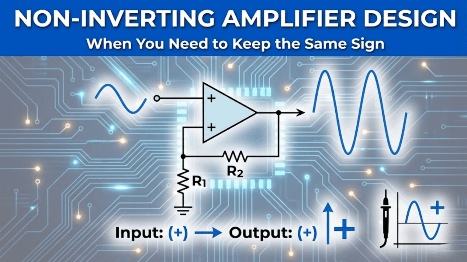
Circuit Topology: Understanding the Non-Inverting Configuration
The non-inverting amplifier consists of:
- The op-amp
- R_f — the feedback resistor, from the output back to the inverting input (V−)
- R_in — the gain-setting resistor, from the inverting input (V−) to ground
The input signal connects directly to the non-inverting input (V+) — no resistor between the signal source and the op-amp input pin. This is the defining characteristic of the non-inverting configuration and the reason for its high input impedance.
The Feedback Network
R_f and R_in form a resistor voltage divider from the output to ground. The junction of this divider — the midpoint between R_f and R_in — connects to the inverting input V−. This means the inverting input always receives a fraction of the output voltage:
V− = V_out × R_in / (R_in + R_f)This voltage divider is the feedback network. It feeds back a scaled version of the output to the inverting input, creating negative feedback that stabilizes the gain.
Why the Signal Goes to V+
The signal connects to V+ (the non-inverting input) rather than through a resistor to V−. This has a profound effect on input impedance:
In the inverting amplifier, V− is held at virtual ground by feedback — so the input resistor R_in connects from the signal to (effectively) ground, giving an input impedance of R_in.
In the non-inverting amplifier, V+ is not held at virtual ground. It’s a free-floating node connected only to the signal source and the op-amp’s input. The op-amp’s non-inverting input has its own very high impedance (megohms to teraohms depending on the input technology). No feedback forces V+ to a fixed voltage — V+ follows whatever the signal source provides.
The result: the non-inverting amplifier’s input impedance is essentially the op-amp’s own differential and common-mode input impedance — hundreds of megohms for BJT inputs, hundreds of gigaohms to teraohms for JFET and MOSFET inputs. For virtually any signal source, this is negligible loading.
The Gain Formula: Derivation and Implications
Deriving the Closed-Loop Gain
Applying the two golden rules of the ideal op-amp:
Rule 1: No current flows into either input terminal.
Rule 2: With negative feedback, V− = V+ = V_in (since V+ is connected directly to the input signal V_in).
The voltage at V− is V_in (from Rule 2). V− is also the midpoint of the R_in / R_f voltage divider from V_out to ground:
V− = V_out × R_in / (R_in + R_f)Since V− = V_in:
V_in = V_out × R_in / (R_in + R_f)Solving for V_out:
V_out / V_in = (R_in + R_f) / R_in = 1 + R_f / R_inClosed-loop gain:
G = 1 + R_f / R_inKey Implications of the Formula
The gain is always ≥ 1. The “+1” term means you cannot make a non-inverting amplifier attenuate — the minimum gain is 1 (achieved when R_f = 0, a short circuit, or when R_in = ∞, an open circuit). If you need attenuation (gain < 1), use the inverting configuration with R_f < R_in, or add an external resistor divider before the non-inverting input.
No phase inversion. The output is in phase with the input. A rising input produces a rising output. The gain formula has no negative sign.
The same resistor ratio — different formula. Comparing to the inverting amplifier (G = −R_f / R_in), the non-inverting formula adds 1 to the ratio. For the same R_f and R_in values, the non-inverting gain is always 1 higher in magnitude than the inverting gain:
- Inverting: G = −10 with R_f = 10kΩ, R_in = 1kΩ
- Non-inverting: G = +11 with the same components
To get non-inverting gain of exactly +10, set R_f = 9 × R_in (not 10 × R_in).
The noise gain equals the closed-loop gain. Unlike the inverting amplifier where noise gain = 1 + R_f/R_in (always higher than the signal gain), the non-inverting amplifier’s noise gain equals its signal gain. This means the bandwidth formula is simpler:
f_−3dB = GBW / G_CL = GBW / (1 + R_f / R_in)The Voltage Follower: The Non-Inverting Amplifier’s Most Important Special Case
When R_f = 0 (a short circuit between output and V−) and R_in = ∞ (open circuit — R_in simply removed), the gain formula becomes:
G = 1 + 0 / ∞ = 1This is the voltage follower — also called a unity-gain buffer, impedance converter, or source follower. The output precisely equals the input: V_out = V_in.
Why the Voltage Follower Is So Useful
A gain of exactly 1 seems trivial. Why would you use an amplifier that doesn’t amplify?
The answer is impedance transformation. The voltage follower:
- Presents extremely high impedance to the source (the op-amp’s input impedance — megohms to teraohms)
- Presents extremely low impedance to the load (near-zero output impedance — milliohms with feedback)
This combination is enormously valuable whenever a high-impedance source must drive a low-impedance load without signal loss.
Concrete example: A pH sensor has an output impedance of 500MΩ. It must drive a 10kΩ display circuit. Without a buffer:
V_load = V_source × R_load / (R_source + R_load)
       = V_source × 10,000 / (500,000,000 + 10,000)
= V_source × 0.002% ≈ 0The sensor signal is completely lost. With a JFET-input voltage follower (Z_in = 10¹²Ω):
V_load = V_source × 10,000 / (10,000 + ~0.001) ≈ V_source × 100%Full signal transfer with negligible loading. The buffer isolates the source from the load entirely.
Other voltage follower applications:
- ADC input buffer: ADC’s sample-and-hold capacitor creates a current spike that would load a high-impedance source without buffering
- Driving long cables: Cable capacitance loads high-impedance sources; a buffer drives the capacitance from its low-impedance output
- Between amplifier stages: Prevents output loading of one stage from affecting the gain of the previous stage
- Reference voltage distribution: A voltage reference (like a Zener or bandgap reference) with limited current output drives multiple loads through a buffer
The Voltage Follower Circuit
The simplest possible op-amp circuit:
- Connect output directly to V− (single wire from output pin to inverting input pin)
- Connect signal to V+
- Connect power supply pins
- Add decoupling capacitors
No resistors needed. The direct output-to-V− connection provides 100% feedback (β = 1), giving the maximum feedback and thus:
- Maximum noise rejection
- Maximum bandwidth (f_−3dB = GBW × 1 = GBW for the buffer)
- Minimum output impedance
- Maximum gain accuracy (G = 1 exactly, to the limit of the ideal model)
Comparing Inverting and Non-Inverting Configurations
Understanding when to use each configuration is a fundamental design decision. The table below summarizes the key differences:
| Property | Inverting Amplifier | Non-Inverting Amplifier |
|---|---|---|
| Gain formula | G = −R_f / R_in | G = 1 + R_f / R_in |
| Gain sign | Negative (inverted) | Positive (non-inverted) |
| Minimum gain | Any (can attenuate) | 1 (cannot attenuate) |
| Input impedance | R_in (set by resistor) | Op-amp’s own Z_in (very high) |
| Noise gain | 1 + R_f / R_in | 1 + R_f / R_in |
| Bandwidth (same G) | Similar (noise gain same) | Similar (noise gain same) |
| Virtual ground | Yes, at V− | No |
| Phase shift | 180° (inverted) | 0° (non-inverted) |
| Input bias error | Compensated by R_comp | R_comp still recommended |
| Summing inputs | Easy (virtual ground) | Not straightforward |
| Input protection | Via series R_in | Needs separate protection resistor |
When to Choose Inverting
- You need attenuation (gain < 1)
- Phase inversion is acceptable or irrelevant (e.g., single audio channel)
- You need a summing amplifier (virtual ground enables multiple inputs)
- Input impedance of R_in is adequate for the source
- You want to use R_in as input protection inherently
- Current-to-voltage conversion (transimpedance amplifier)
When to Choose Non-Inverting
- Phase inversion would cause problems (control systems, matched channels, sensor interfaces)
- Source impedance is very high (pH electrodes, piezo sensors, electret microphones)
- You need gain exactly ≥ 1 and want to avoid a separate buffer
- You want maximum input impedance with minimum components (especially as a buffer/follower)
- Cascading stages where loading between stages is a concern
- Single-supply circuits where input signal is already at a convenient DC level
In many real designs, both configurations appear in the same circuit, each used where its properties are most advantageous.
Component Selection for the Non-Inverting Amplifier
Resistor Value Guidelines
The same general range (1kΩ to 1MΩ) applies as for the inverting amplifier, but with some differences in emphasis:
R_in lower limit: R_in connects from V− to ground. It must not be so small that it overloads the feedback voltage divider (draws excessive current from the output) or creates a noise floor higher than the op-amp’s own noise. Values below 1kΩ are rarely needed.
R_in upper limit: Very large R_in values (>1MΩ) combined with the op-amp’s input capacitance create a pole at the non-inverting input that can affect high-frequency performance. More importantly, large R_in values interact with input bias current to create DC errors even though R_in is connected to ground (not to a high-impedance source).
For gains near 1: When R_f / R_in << 1 (low gain), the ratio accuracy matters more than absolute values. Use resistors from the same batch or matched values for best gain accuracy. For a gain of 1.1 (R_f = 1kΩ, R_in = 10kΩ), a 1% error in the ratio causes a 10% error in the fractional gain above 1 — the total gain error is 1% of 0.1, or 0.1%.
For high gains: As with the inverting amplifier, keeping R_f ≤ 100kΩ minimizes Johnson noise and stray capacitance effects. For gain 100: choose R_in = 1kΩ, R_f = 99kΩ (use 100kΩ for G ≈ 101, or 98.7kΩ standard value for closer accuracy).
Setting Exact Gain Values
The “+1” in the non-inverting gain formula sometimes makes hitting exact gain targets slightly awkward. Here are useful relationships:
For a target gain G:
R_f / R_in = G − 1So:
- Gain 2: R_f / R_in = 1 → R_f = R_in (any equal value pair)
- Gain 5: R_f / R_in = 4 → R_f = 4 × R_in (e.g., 10kΩ and 40kΩ)
- Gain 10: R_f / R_in = 9 → R_f = 9 × R_in (e.g., 10kΩ and 90kΩ, or 5.6kΩ and 51kΩ)
- Gain 11: R_f / R_in = 10 → R_f = 10kΩ, R_in = 1kΩ (coincidentally clean ratio)
- Gain 20: R_f / R_in = 19 → Not a standard ratio — use 19.1kΩ and 1kΩ (E96 series) or 18kΩ + 1kΩ in series for R_f
For non-standard gain targets, two approaches work well:
- Use E96 series (1% tolerance) resistors which cover more values: 19.1kΩ and 1kΩ give G = 1 + 19.1 = 20.1 (0.5% error from G = 20)
- Use a combination of series/parallel resistors: (18kΩ + 1kΩ) in series with 1kΩ gives R_f = 19kΩ, G = 20 exactly with standard values
Bias Current Compensation Resistor
Even though R_in is connected to ground (not a high-impedance signal node), the non-inverting input is connected directly to the signal source through zero resistance. The bias current of the non-inverting input flows through the source impedance of the signal source.
The compensation approach is identical to the inverting amplifier: add R_comp = R_f ∥ R_in at the appropriate location. But now R_comp goes in series with the non-inverting input (between the signal source and V+), while the inverting input already sees R_f ∥ R_in through the feedback network.
R_comp = R_f ∥ R_in = (R_f × R_in) / (R_f + R_in)Important: R_comp in series with V+ creates a low-pass filter with any capacitance at V+ (including the op-amp’s input capacitance of ~2pF). Keep R_comp small (below 10kΩ) to keep this pole above the signal bandwidth:
f_pole = 1 / (2π × R_comp × C_in)For R_comp = 10kΩ and C_in = 2pF: f_pole = 1 / (2π × 10,000 × 2×10⁻¹²) = 7.96MHz — well above audio. For R_comp = 1MΩ: f_pole = 79.6kHz — problematic for high-frequency signals.
For JFET-input op-amps, bias current is in the picoamp range and R_comp is usually omitted. For BJT-input op-amps (like NE5532), include R_comp.
Bandwidth, Stability, and the Unity-Gain Challenge
Bandwidth Calculation
The closed-loop bandwidth of the non-inverting amplifier:
f_−3dB ≈ GBW / G_CL = GBW / (1 + R_f / R_in)This is identical in form to the inverting case. The bandwidth decreases as gain increases — a fundamental tradeoff of the gain-bandwidth product.
Worked example: NE5532 (GBW = 10MHz), gain = 20:
f_−3dB = 10MHz / 20 = 500kHz — ample for audio ✓Worked example: TL071 (GBW = 3MHz), gain = 100:
f_−3dB = 3MHz / 100 = 30kHz — marginal for audio (20kHz required)Rule of thumb: choose op-amp GBW ≥ 10 × (G_CL × f_signal_max) for comfortable margin.
The Unity-Gain Stability Challenge
The voltage follower (G = 1) operates at maximum feedback (β = 1, 100% of output returned to input). This maximum feedback is also the most challenging condition for stability.
Why? Stability requires that when the signal goes around the feedback loop, the total phase shift is less than 180° when the loop gain exceeds 1. With 100% feedback (β = 1), the loop gain is highest, and the loop stays gain > 1 to higher frequencies — where more phase shift has accumulated. If the op-amp has insufficient phase margin at unity gain, the voltage follower oscillates.
Most general-purpose op-amps are unity-gain stable — they are internally compensated to remain stable even at G = 1. This compensation (the internal dominant pole capacitor) is the reason their bandwidth starts rolling off at such low frequencies (sometimes as low as 10Hz open-loop).
However, some high-speed op-amps are only stable at gains above 5 or 10. These “decompensated” op-amps trade away unity-gain stability for higher bandwidth at higher gains. Their datasheets specify a minimum stable gain. Never use a decompensated op-amp as a voltage follower — it will oscillate. Examples: AD8055 (minimum stable gain = 2), LM7171 (minimum stable gain = 10).
Capacitive Load Stability
The voltage follower is particularly sensitive to capacitive loads. A capacitive load (cable capacitance, ADC input capacitance, power bypass capacitors accidentally connected to the output) creates a pole in the feedback loop that adds phase shift. Combined with the high loop gain at unity, this can cause oscillation.
The standard fix: add a small series resistor (10Ω to 100Ω) between the op-amp output and the load. This isolates the capacitive load from the op-amp, removing the phase-shifting pole from inside the feedback loop. The output voltage at the op-amp output pin is still well-regulated by feedback; the small resistor’s voltage drop is negligible at low frequencies.
For driving long cables (which have significant capacitance — typically 100pF/meter), a series 50Ω resistor is standard practice for voltage followers. The resistor matches the cable impedance and prevents reflections while also stabilizing the feedback loop.
DC Offset in the Non-Inverting Amplifier
The same sources of DC offset appear in both inverting and non-inverting configurations.
Output Offset Due to V_OS
The input offset voltage is amplified by the noise gain (= closed-loop gain for non-inverting):
V_out_error (from V_OS) = V_OS × G_CL = V_OS × (1 + R_f / R_in)This formula is identical to the inverting amplifier case. The non-inverting amplifier offers no advantage over inverting for offset voltage.
Output Offset Due to Input Bias Current
The bias current of the non-inverting input flows through the source impedance of the signal source (plus R_comp if present). For a sensor with source impedance Z_source:
V_out_error (from I_B+) = I_B+ × (Z_source + R_comp) × G_CLThis is why high-impedance sources with BJT-input op-amps can produce large output offsets — the bias current creates a voltage drop across the high source impedance, and that voltage is amplified by the full closed-loop gain.
Example: pH electrode (Z_source = 500MΩ), LM741 (I_B = 80nA), gain 10:
V_out_error = 80nA × 500MΩ × 10 = 80×10⁻⁹ × 5×10⁸ × 10 = 400VObviously impossible — the output would saturate at the supply rail. This illustrates why JFET or MOSFET input op-amps are mandatory for high-impedance sources. With TL071 (I_B = 30pA):
V_out_error = 30pA × 500MΩ × 10 = 30×10⁻¹² × 5×10⁸ × 10 = 0.15VStill significant at gain 10. For pH measurement (millivolt signals), use an ultra-low bias current amplifier like LMC6001 (I_B = 25fA):
V_out_error = 25fA × 500MΩ × 10 = 25×10⁻¹⁵ × 5×10⁸ × 10 = 125µVAcceptable for most pH measurements.
Single-Supply Non-Inverting Amplifier
Operating from a single supply is straightforward with the non-inverting configuration because the signal applies directly to V+, making biasing explicit and intuitive.
Biasing for Single Supply
The signal must be centered within the op-amp’s input common-mode range. For a 5V single supply, the input should be centered near VCC/2 = 2.5V. This biasing is accomplished either:
By the signal source itself: If the signal is already centered on 2.5V (e.g., from another single-supply stage), no additional biasing is needed.
By an external bias network: A resistor divider (two equal resistors from 5V to GND, junction = 2.5V) connects to V+ through a large resistor (R_bias, typically 100kΩ), and the signal couples through a capacitor to the same node. R_bias is large so it doesn’t load the divider but provides a DC path for bias current.
The R_bias interacts with the input capacitance of the op-amp and the source capacitor to set the low-frequency cutoff — ensure these values are chosen to keep the low-frequency cutoff below the signal band.
Output Swing Considerations
With a single 5V supply, the output ideally swings from 0V to 5V. In practice:
- Standard op-amps (LM358): output swings from ~1V to ~3.5V — only 2.5V range from a 5V supply
- Rail-to-rail output op-amps (MCP6002, OPA314): output swings from ~10mV to ~4.99V — nearly the full 5V
For best single-supply performance at 3.3V or 5V, always use rail-to-rail output op-amps.
Practical Design Examples
Design Example 1: High-Impedance Electret Microphone Preamplifier
Application: Amplify an electret microphone capsule output. Electret capsules have very high source impedance (typically 1–10kΩ for the internal FET output, but the DC biasing resistor should not load the signal). The capsule needs a DC bias current (typically 0.5mA) supplied through a resistor from VCC.
Specifications:
- Gain: +20 (26dB)
- Frequency: 100Hz – 15kHz
- Supply: ±9V dual
- Non-inverting (signal polarity matters for later DSP processing)
Op-amp selection: TL071 — JFET input (low bias current won’t disturb microphone biasing), low noise for audio, GBW = 3MHz, ±9V supply suitable.
Bandwidth verification:
f_−3dB = 3MHz / 20 = 150kHz >> 15kHz ✓Resistor selection for gain 20:
R_f / R_in = G − 1 = 20 − 1 = 19Choose R_in = 5.1kΩ, R_f = 97kΩ (use 100kΩ for G = 1 + 100/5.1 = 20.6, acceptable) Or: R_in = 4.7kΩ, R_f = 91kΩ → G = 1 + 91/4.7 = 20.4 ✓ (standard E24 values)
Bias compensation:
R_comp = R_f ∥ R_in = (91,000 × 4,700) / (91,000 + 4,700) = 4,468Ω → use 4.7kΩPlace R_comp between signal source and V+.
Input coupling capacitor: C_in in series with microphone → R_comp → V+, blocking DC from microphone bias circuit. C_in = 10µF (film or electrolytic, observe polarity): f_low = 1 / (2π × R_comp × C_in) ≈ 3.4Hz — well below 100Hz ✓
Output coupling (if AC output desired): C_out = 10µF in series with output, forming high-pass with load impedance.
Design Example 2: Precision Voltage Buffer for Reference Distribution
Application: A precision 2.500V voltage reference (ADR4525) with 5mA maximum output current must drive ten parallel 1kΩ loads (total 100Ω, requiring 25mA) without degrading its accuracy. Use a voltage follower buffer.
Analysis without buffer: Reference output impedance ≈ 10Ω. With 100Ω load:
V_load = 2.500 × 100/(100+10) = 2.273V — 9% error, unacceptableWith voltage follower buffer: Op-amp input draws < 1nA (JFET type), negligible loading of reference. Op-amp output impedance with feedback ≈ 0.01Ω. Output current requirement: 2.5V / 100Ω = 25mA — need op-amp with ≥ 25mA output capability.
Op-amp selection: OPA2134 (JFET input, low noise, 40mA output current, low offset for precision reference buffering).
Circuit:
- ADR4525 output → 100Ω (isolation between reference and op-amp input — optional but good practice) → V+
- V− connected directly to output (voltage follower)
- 100nF + 10µF decoupling on each supply pin
- Small 10Ω resistor between op-amp output and load (capacitive load stability — multiple parallel loads have combined capacitance)
Resulting accuracy: V_OS of OPA2134 = 500µV max → V_out_error = 500µV × 1 = 500µV = 0.02% — acceptable for most precision reference applications. For tighter accuracy, use OP2177 (V_OS = 60µV max → 0.0024% error).
Design Example 3: Instrumentation-Quality Gain Stage for Wheatstone Bridge
Application: A Wheatstone bridge strain gauge produces 1mV/V excitation at full scale. With a 5V excitation, full-scale output = 5mV differential. Amplify single-ended bridge output to 0–4V for a 5V ADC. Required gain ≈ 800.
Challenge: Gain 800 requires careful op-amp selection. A single non-inverting stage at gain 800 with a 1MHz GBW op-amp gives:
f_−3dB = 1MHz / 800 = 1.25kHzAdequate for slow strain measurements (DC to 100Hz), but bandwidth is tight.
For gain 800 in a single stage:
R_f / R_in = 799Choose R_in = 124Ω (E96), R_f = 100kΩ → G = 1 + 100,000/124 = 807 ≈ 800 (1% high) Or: R_in = 125Ω (E96), R_f = 100kΩ → G = 1 + 100,000/125 = 801 ✓
Op-amp selection: INA128 instrumentation amplifier (a dedicated three-op-amp instrumentation amplifier) would normally be preferred for bridge measurements — but for a single-ended non-inverting design, use AD8221 or OP07 for low offset.
Using OP07 (V_OS = 25µV max, I_B = 4nA, GBW = 0.6MHz):
Bandwidth: 0.6MHz / 800 = 750Hz — adequate for quasi-static strain measurement.
Output offset:
V_out_error = V_OS × G = 25µV × 800 = 20mV (referred to output) = 25µV referred to inputFor a 5mV full-scale input signal, 25µV input-referred error = 0.5% — acceptable for many applications.
Alternative two-stage approach for better bandwidth: Stage 1 (non-inverting): Gain = 40, bandwidth = 0.6MHz/40 = 15kHz ✓ Stage 2 (non-inverting or inverting): Gain = 20, bandwidth = 0.6MHz/20 = 30kHz ✓ Total gain = 40 × 20 = 800 ✓, bandwidth = 15kHz (limited by first stage)
Two stages provide the same total gain with 12× better bandwidth than a single stage, at the cost of one more op-amp and resistor set.
Design Example 4: Single-Supply Audio Amplifier (5V System)
Application: Amplify audio from a DAC (0–3.3V range, centered on 1.65V) for driving a small speaker through a class-D amplifier. Need non-inverting gain of 2 to boost 1.65V ± 0.8V signal to 1.65V ± 1.6V range.
Specifications:
- Gain: +2 (6dB)
- Supply: 5V single
- Frequency: 20Hz – 20kHz
- Rail-to-rail operation needed
Op-amp selection: MCP6002 — 1.8V to 5.5V supply, rail-to-rail I/O, GBW = 1MHz, SOT-23 or DIP-8 package.
Bandwidth:
f_−3dB = 1MHz / 2 = 500kHz >> 20kHz ✓Resistor selection (gain 2):
R_f / R_in = G − 1 = 1
R_f = R_in → use R_f = R_in = 10kΩDC biasing: DAC output is already centered on 1.65V (VCC/2). No additional biasing needed for V+. The output will center on 1.65V × 2 − 1.65V × 1 = 1.65V…
Wait — let’s verify. With V+ = 1.65V + 0.8V×sin(ωt):
V_out = G × V_in = 2 × (1.65 + 0.8×sin(ωt)) = 3.3 + 1.6×sin(ωt)Output swings between 3.3 − 1.6 = 1.7V and 3.3 + 1.6 = 4.9V. Both within 5V rail. ✓
Circuit note: Ensure R_in is connected from V− to ground (not to VCC/2). The non-inverting input receives the DAC signal directly. R_f returns the output to V−. This keeps the circuit simple — no mid-supply biasing needed since the input is already at the right level.
Design Example 5: Variable-Gain Non-Inverting Amplifier
Application: Adjustable gain from ×1 to ×11 with a potentiometer, for a volume control or calibration adjustment.
Concept: Replace R_in with a fixed resistor R_min in series with a potentiometer R_pot:
G = 1 + R_f / (R_min + R_pot_wiper)When R_pot = 0: G_max = 1 + R_f / R_min When R_pot = R_pot_max: G_min = 1 + R_f / (R_min + R_pot_max)
Design for G = 1 to 11:
Choose R_f = 100kΩ.
At G_max = 11: R_min = R_f / (G_max − 1) = 100kΩ / 10 = 10kΩ (with R_pot = 0) At G_min = 1: Requires R_f / (R_min + R_pot_max) → 0, meaning R_min + R_pot_max → ∞
But G = 1 exactly requires no feedback division — i.e., R_in → ∞. With finite R_pot_max:
G_min = 1 + 100,000 / (10,000 + R_pot_max)For G_min ≈ 1.1 (10% above unity), set R_pot_max = 1MΩ:
G_min = 1 + 100,000 / (10,000 + 1,000,000) = 1 + 0.099 = 1.099 ≈ 1.1So with R_f = 100kΩ, R_min = 10kΩ, and R_pot = 1MΩ:
- Pot at minimum (0Ω): G = 1 + 100k/10k = 11 ✓ (maximum gain)
- Pot at maximum (1MΩ): G = 1 + 100k/1.01M = 1.099 ≈ 1.1 (near-unity gain)
Note: gain varies nonlinearly with potentiometer position because it’s a function of 1/(R_min + R_pot). For a more linear-feeling control, use a logarithmic (audio taper) potentiometer.
Op-amp choice: Any unity-gain-stable op-amp. For audio, NE5532 (low noise). For general-purpose, TL071 or MCP6002. For precision, OP27.
Layout and Construction Best Practices
Input Protection for the Non-Inverting Configuration
Because the signal source connects directly to V+ with no series resistor, the non-inverting input is more vulnerable to overvoltage than the inverting input (where R_in provides inherent current limiting).
Add a series protection resistor (R_prot = 1kΩ to 10kΩ) between the signal source and V+. This limits current through the op-amp’s internal ESD protection diodes if the input exceeds the supply rails. The resistor’s effect on bandwidth: combined with the op-amp’s input capacitance (~2pF), it creates a pole at:
f_pole = 1 / (2π × R_prot × C_in)For R_prot = 10kΩ, C_in = 2pF: f_pole = 7.96MHz — no issue for audio or low-frequency applications.
For applications where the pole matters (RF, high-speed), use a smaller protection resistor (100Ω to 1kΩ) or use Schottky clamping diodes instead.
Feedback Capacitor for High-Frequency Stability
At high gains with large R_f values, stray capacitance at the V− node (op-amp pin capacitance plus PCB pad capacitance, typically 1–5pF) in parallel with R_f creates a pole that reduces feedback at high frequencies. At the frequency where this pole sits, the circuit may have insufficient phase margin and oscillate.
The solution is to add a small capacitor C_f (1pF to 47pF) in parallel with R_f (between output and V−). This creates a zero in the feedback transfer function that compensates for the pole from stray capacitance. The optimal C_f:
C_f ≈ 1 / (2π × R_f × f_unity)Where f_unity is the op-amp’s unity-gain bandwidth (GBW). For R_f = 100kΩ and GBW = 3MHz:
C_f ≈ 1 / (2π × 100,000 × 3,000,000) = 0.53pFIn practice, use 1pF to 5pF and verify stability on the bench. If the output shows ringing or oscillation at high frequencies, increase C_f in small steps (1pF, 2pF, 3.3pF, 4.7pF, 10pF) until the ringing disappears.
Troubleshooting Non-Inverting Amplifier Circuits
Problem: Output is stuck at supply rail (saturated)
- Feedback disconnected: R_f from output to V− must be present and connected correctly.
- Feedback accidentally going to V+ (positive feedback) — check R_f goes to the inverting input, not the non-inverting.
- Input common-mode range exceeded: V+ voltage outside the op-amp’s specified range. Check input voltage vs. datasheet.
- Using a decompensated op-amp as unity-gain follower — it oscillates and appears saturated. Verify op-amp is unity-gain stable or add minimum gain.
Problem: Large DC offset at output
- V_OS × G_CL effect — normal for high gains. Use precision op-amp or add offset null trimmer.
- R_comp missing or wrong value — verify R_comp = R_f ∥ R_in placed in series with V+.
- Bias current through source impedance — significant for BJT inputs with high-impedance sources. Use JFET/MOSFET input op-amp.
Problem: Output oscillates at high frequency
- Missing decoupling capacitors. Add 100nF ceramics to each supply pin within 5mm of the IC.
- Capacitive load (cable or ADC input) causing instability in voltage follower. Add 50–100Ω series resistor between op-amp output and load.
- R_f too large. Add small C_f (1–10pF) in parallel with R_f.
- Decompensated op-amp used below minimum stable gain. Check datasheet minimum gain specification.
Problem: Gain lower than expected at high frequencies
- Signal frequency approaching GBW / G_CL. Either reduce gain, use higher-GBW op-amp, or accept bandwidth limitation.
- Output clipping (input amplitude too large). Reduce input or reduce gain.
- Slew rate limitation for large-amplitude, high-frequency signals. Choose op-amp with higher slew rate.
Problem: Signal attenuation (gain below 1)
- Impossible with a non-inverting amplifier (gain is always ≥ 1). If signal is being attenuated, the circuit is wired as an inverting amplifier (input on V−) or the feedback network is connected incorrectly. Re-examine wiring.
Summary
The non-inverting amplifier is the essential op-amp circuit when phase preservation and high input impedance are required. Its gain G = 1 + R_f / R_in is always positive (no phase inversion) and always ≥ 1 (cannot attenuate). The signal applies directly to V+, presenting the op-amp’s own very high input impedance — megohms to teraohms — to the signal source.
The voltage follower (G = 1, R_f = 0, R_in removed) is the most important special case: it transfers voltage from a high-impedance source to a low-impedance load with perfect fidelity, consuming no signal in the process. Every analog circuit chain that interfaces high-impedance sources to processing stages uses voltage followers as the first stage.
Key design considerations mirror those of the inverting amplifier: keep resistors in the 1kΩ–100kΩ range for noise and bandwidth; add R_comp = R_f ∥ R_in in series with V+ for bias current compensation with BJT-input op-amps; verify bandwidth against GBW / G_CL; use unity-gain stable op-amps for voltage follower applications; add series output resistor (50–100Ω) when driving capacitive loads.
Single-supply designs require rail-to-rail op-amps (MCP6002, LMV321) and careful attention to input biasing and output swing. High-impedance sources (pH electrodes, piezo sensors, electret microphones) require JFET or MOSFET input op-amps (TL071, LMC6001) to avoid bias-current-induced offset errors.
Together, the inverting and non-inverting amplifier configurations cover the full range of signal amplification needs in analog electronics. Knowing their properties, tradeoffs, and design procedures gives you a powerful toolkit for building virtually any analog signal processing circuit.