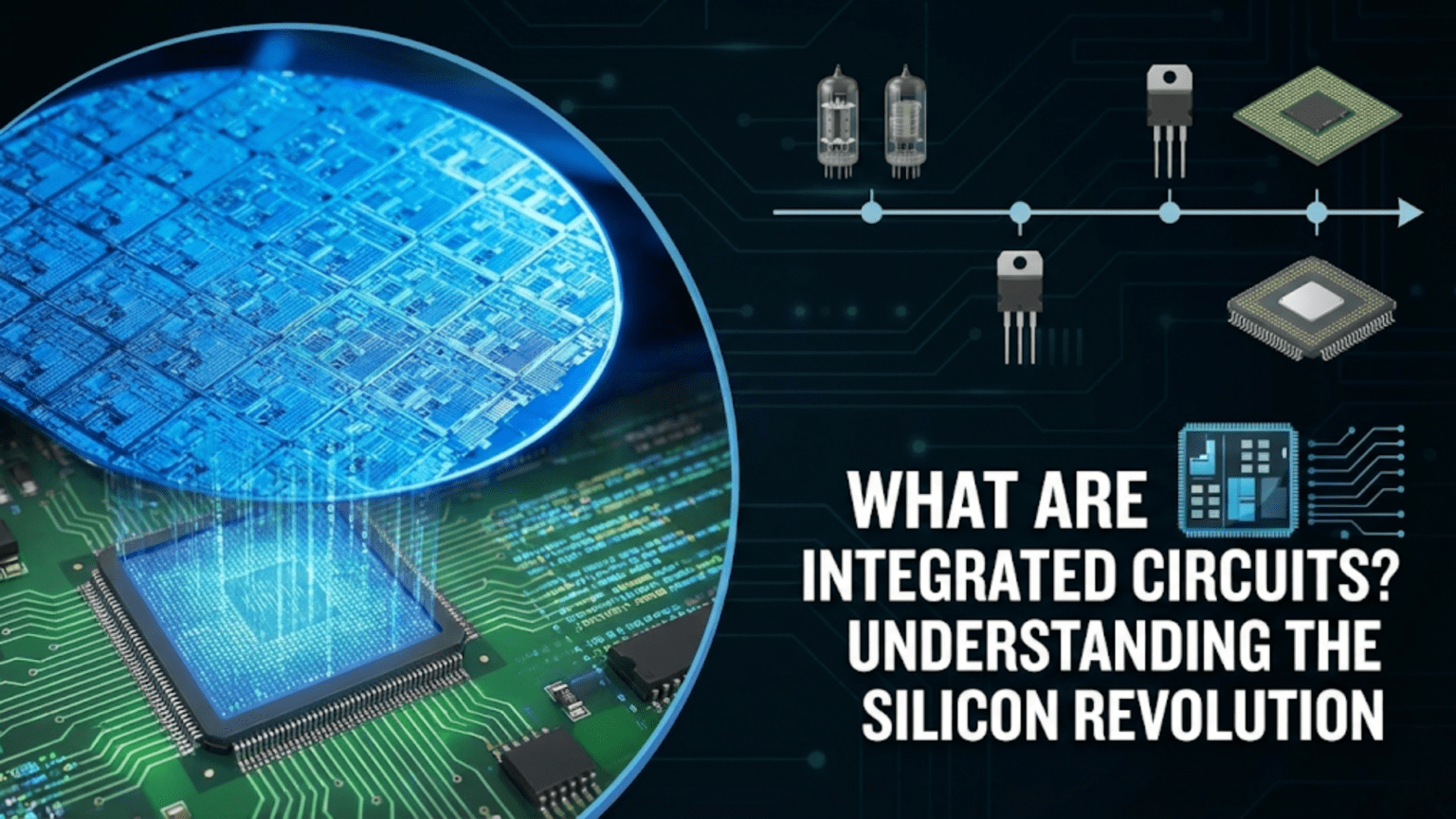
An integrated circuit (IC) is a miniaturized electronic circuit containing transistors, resistors, capacitors, and other components fabricated onto a small chip of semiconductor material — typically silicon. These tiny chips revolutionized electronics by packing thousands to billions of components into a space smaller than a fingernail, enabling everything from smartphones to spacecraft.
Introduction: The Tiny Chip That Changed the World
Imagine trying to build a modern smartphone using individual electronic components. Each transistor would need to be wired by hand, each resistor soldered into place, each capacitor mounted on a board. A device with the processing power of today’s smartphone would require a structure the size of a football field — and consume enough electricity to power a small city.
This was the reality of early electronics. In the 1940s and 1950s, computers like ENIAC filled entire rooms, required teams of engineers to maintain, and still performed calculations far slower than the chip inside a modern wristwatch. The bottleneck wasn’t imagination or engineering talent — it was the physical limitation of building circuits from discrete, individually manufactured components.
The integrated circuit changed everything.
By etching entire circuits — transistors, resistors, capacitors, and their interconnections — directly onto a single piece of silicon, engineers compressed what once filled rooms into chips smaller than your thumbnail. This innovation didn’t just make electronics smaller; it made them faster, cheaper, more reliable, and accessible to everyone.
Today, integrated circuits are everywhere. They process your phone calls, control your car’s engine, regulate the temperature in your refrigerator, display images on your screen, and execute billions of calculations per second in the device you’re reading this on right now. Understanding what integrated circuits are, how they work, and why they matter is fundamental to understanding modern electronics.
This article takes you from the basic concept of an IC through its internal structure, manufacturing process, types, real-world applications, and practical tips for working with them. Whether you’re just starting out in electronics or looking to solidify your foundational knowledge, this guide will give you a thorough understanding of one of humanity’s most transformative inventions.
The Problem That Integrated Circuits Solved
To truly appreciate the integrated circuit, you need to understand the world before it existed.
The Era of Discrete Components
Before ICs, every electronic circuit was built from individual, discrete components — each one manufactured separately and then connected together by hand. A simple radio receiver might require dozens of components: vacuum tubes (later transistors), resistors, capacitors, coils, and the wires connecting them all. An early computer required thousands.
This created several serious problems:
Size: Each component occupied physical space. As circuit complexity grew, the physical size of the device grew proportionally. There was no practical way to miniaturize beyond the size of the smallest individual component.
Reliability: Every solder joint, every wire connection, every component was a potential failure point. A circuit with ten thousand components had ten thousand places where something could go wrong. Early computers failed so frequently that engineers spent more time repairing them than using them.
Speed: Electrical signals traveling through wires between discrete components encounter resistance, capacitance, and inductance that limit how fast signals can move. The longer the wires, the slower the circuit.
Cost: Each component had to be manufactured, tested, shipped, purchased, and hand-assembled. Labor costs alone made complex electronics extraordinarily expensive.
Power consumption: Every connection, every wire, every component junction consumed power. Large circuits with long wires wasted significant energy.
These limitations created a ceiling — a point beyond which electronics simply couldn’t advance without a fundamental rethinking of how circuits were built.
The Tyranny of Numbers
In 1958, Jack Kilby at Texas Instruments and Robert Noyce at Fairchild Semiconductor (working independently) identified the core problem: the tyranny of numbers. Complex electronics required huge numbers of components, and assembling those components by hand was expensive, slow, and unreliable.
Their insight was revolutionary: instead of manufacturing components separately and connecting them afterward, why not manufacture the entire circuit — components and connections — at once, on a single piece of semiconductor material?
This was the integrated circuit. Both men are credited as co-inventors (Kilby received the Nobel Prize in Physics in 2000; Noyce passed away before the prize could be awarded posthumously).
What Exactly Is an Integrated Circuit?
An integrated circuit, also called a chip, microchip, or IC, is a complete electronic circuit fabricated on a single piece of semiconductor material — almost always silicon.
The key word here is “integrated.” Rather than assembling separate components and connecting them with wires, an IC integrates all the components and their connections into a single, monolithic structure. The transistors, resistors, capacitors, and the metal pathways connecting them are all formed simultaneously through a series of manufacturing steps performed on the same piece of silicon.
The Basic Structure
A complete integrated circuit consists of three layers of structure:
The die: This is the actual silicon chip — a tiny rectangle, typically a few millimeters on each side, containing all the fabricated components. Under a microscope, the die looks like an incredibly intricate city of miniature structures.
The package: The die is fragile and has microscopic connection points that can’t be handled directly. The package is a protective housing — usually plastic or ceramic — that encases the die and extends its connections to large, solderable pins or pads that humans (and pick-and-place machines) can work with.
The bond wires: Inside the package, ultrathin gold or aluminum wires connect the die’s tiny contact pads to the package’s larger pins. These wires are so thin they’re nearly invisible to the naked eye.
When you hold an IC in your hand, you’re holding the package. The actual silicon chip inside might be smaller than a grain of rice. The package might be a DIP (Dual Inline Package) with two rows of pins, a SOIC (Small Outline IC) for surface-mount applications, a QFP (Quad Flat Package) with pins on all four sides, or any number of other form factors.
What’s Inside: The Components
An IC contains the same basic electronic components found in discrete circuits — just fabricated in a radically different way.
Transistors are the workhorses of integrated circuits. In a modern microprocessor, there may be tens of billions of transistors on a chip the size of a thumbnail. Each transistor is a three-terminal semiconductor device that can act as a switch or amplifier. In digital ICs, transistors are used as switches — either fully on or fully off. In analog ICs, they operate in their linear region for amplification.
Resistors in integrated circuits are formed by creating regions of lightly doped silicon — silicon with fewer charge-carrying impurities. The resistance of these regions can be controlled by adjusting the doping concentration and the physical dimensions of the region. IC resistors are less precise than discrete resistors and have limited resistance ranges, which is why designers often prefer to use transistor-based circuits (like current mirrors) to create controllable currents rather than relying on resistors.
Capacitors in ICs are typically formed either by the reverse-biased junction between doped silicon regions (junction capacitors) or by a thin oxide layer sandwiched between conductors (MOS capacitors). IC capacitors are physically small and have limited capacitance values — this is why you’ll notice that most ICs require external capacitors (like decoupling capacitors) for functions requiring larger capacitance.
Diodes are formed by creating junctions between p-type and n-type silicon regions — essentially transistors with two terminals connected together. They’re used for protection, voltage clamping, and in analog circuits.
Interconnects are the metal pathways connecting components. Modern ICs use multiple layers of metal (often aluminum or copper) separated by insulating layers, allowing connections to route over and under each other without short-circuiting.
How Integrated Circuits Are Made
The manufacturing of integrated circuits — called semiconductor fabrication or “fab” — is one of the most complex industrial processes humans have ever developed. Modern IC fabrication takes place in cleanrooms so pure that the air contains fewer particles per cubic meter than outer space. The processes involved operate at scales measured in nanometers — billionths of a meter.
The Starting Material: Silicon Wafers
It begins with silicon dioxide — ordinary sand. Silicon is purified to an extraordinary degree (99.9999999% pure, sometimes called “nine nines pure”) and grown into large single-crystal cylinders called ingots, using a process called the Czochralski process. These ingots are sliced into thin discs called wafers, typically 200mm or 300mm in diameter and less than a millimeter thick. Each wafer will eventually contain hundreds or thousands of identical chips.
The Photolithography Process
The core manufacturing technique is photolithography — a process borrowed from photography. Here’s a simplified overview:
- Oxidation: The silicon wafer is exposed to oxygen at high temperature, growing a thin layer of silicon dioxide on its surface.
- Photoresist coating: A light-sensitive polymer called photoresist is spin-coated onto the wafer surface.
- Exposure: A mask — essentially a template containing the circuit pattern — is placed over the wafer, and ultraviolet light (or in modern fabs, extreme ultraviolet light) is shone through it. The light changes the chemical properties of the photoresist where it hits.
- Development: The wafer is treated with a developer solution that dissolves either the exposed or unexposed photoresist, leaving a patterned layer.
- Etching: Chemicals or plasma etch away the exposed silicon dioxide, transferring the pattern into the silicon surface.
- Ion implantation: Dopant atoms (impurities that modify silicon’s electrical properties) are fired into specific regions of the silicon to create p-type and n-type regions.
This process is repeated dozens of times with different masks to build up the layers of transistors, insulators, and metal interconnects that form the complete circuit.
The Scale of Modern Manufacturing
Modern chips are manufactured at process nodes measured in nanometers. As of the early 2020s, leading-edge processors use 3nm to 5nm process nodes — meaning the smallest features on the chip are just a few nanometers across. For context, a human hair is about 70,000 nanometers wide. A single transistor in a modern processor is smaller than a virus.
This incredible miniaturization is what makes modern electronics possible. The more transistors you can fit on a chip, the more processing power and functionality you can achieve in the same physical space.
Wafer Testing and Dicing
After fabrication, each chip on the wafer is tested automatically using probe cards — arrays of tiny needles that contact the chip’s test pads. Failed chips are marked. The wafer is then diced — cut into individual chips using a diamond saw or laser. Good chips are packaged; failed chips are discarded.
Types of Integrated Circuits
Integrated circuits span an enormous range of functionality, from simple logic gates to complete computer systems. They’re broadly categorized by their function and complexity.
Analog Integrated Circuits
Analog ICs process continuous signals — voltages and currents that can take any value within a range. They’re used wherever real-world signals need to be amplified, filtered, converted, or compared.
Operational amplifiers (op-amps) are the most fundamental analog building blocks. A single op-amp IC like the classic LM741 or the modern TL071 contains a complete differential amplifier circuit with tens of transistors, yet costs pennies. Op-amps are used for signal amplification, filtering, mathematical operations, and comparator functions.
Voltage regulators like the LM7805 contain complete linear regulation circuits — including a voltage reference, error amplifier, pass transistor, and protection circuitry — in a single three-pin package. These ICs accept a range of input voltages and provide a stable, regulated output regardless of load current variations.
Comparators compare two input voltages and output a digital signal indicating which is higher. While op-amps can be used as comparators, dedicated comparator ICs like the LM393 are optimized for speed and have open-collector outputs suitable for driving digital logic.
Analog-to-digital converters (ADCs) and digital-to-analog converters (DACs) bridge the analog and digital worlds, converting real-world signals into digital numbers and vice versa. These ICs are found in every audio system, measurement instrument, and sensor interface.
Digital Integrated Circuits
Digital ICs operate with discrete signal levels — high and low, representing 1s and 0s. They’re the foundation of all computing and digital communication.
Logic gates are the simplest digital ICs. A 74HC00, for example, contains four NAND gates in a single 14-pin package. These gates implement Boolean logic operations — AND, OR, NOT, NAND, NOR, XOR — that form the building blocks of all digital circuits.
Flip-flops and registers store binary data. A 74HC74 contains two D-type flip-flops — basic memory cells that remember a single bit of information. String these together and you have registers, counters, and memory arrays.
Microcontrollers integrate a processor core, memory, and peripheral circuits (like ADCs, timers, and communication interfaces) on a single chip. An Arduino’s ATmega328P microcontroller contains 32KB of program memory, 2KB of RAM, a CPU, timers, a 10-bit ADC, and multiple communication interfaces in a package smaller than a postage stamp.
Microprocessors are the computing hearts of computers and smartphones. A modern AMD or Intel processor contains tens of billions of transistors implementing instruction decoders, arithmetic units, cache memory, and control logic.
Memory chips — RAM, ROM, Flash — store digital information. A USB flash drive contains NAND Flash memory chips that store billions of bits of data in a structure of floating-gate transistors.
FPGAs (Field-Programmable Gate Arrays) are programmable digital ICs containing arrays of logic blocks that can be configured by the user to implement any digital circuit. They’re used in prototyping, signal processing, and applications requiring custom digital logic.
Mixed-Signal Integrated Circuits
Many real-world applications require both analog and digital functions. Mixed-signal ICs integrate both on the same chip.
System-on-Chip (SoC) devices like those in smartphones combine a CPU, GPU, memory controllers, wireless radios, audio codecs, image processors, and power management — all analog and digital — on a single die.
Audio codecs contain ADCs to digitize microphone input, DACs to drive speakers, and digital processing to implement filters and effects.
Power management ICs (PMICs) combine multiple switching regulators, linear regulators, battery chargers, and voltage supervisors for complete power system management in portable devices.
The Scale of Integration: From SSI to ULSI
Integrated circuits are also classified by their scale of integration — how many components they contain.
| Scale | Abbreviation | Component Count | Example |
|---|---|---|---|
| Small-Scale Integration | SSI | 1–10 gates | 7400 NAND gate |
| Medium-Scale Integration | MSI | 10–100 gates | 74HC595 shift register |
| Large-Scale Integration | LSI | 100–10,000 gates | Z80 processor (1976) |
| Very Large-Scale Integration | VLSI | 10,000–1M gates | Intel 80386 (1985) |
| Ultra Large-Scale Integration | ULSI | >1M transistors | Modern CPUs (>10 billion) |
The progression from SSI to ULSI represents the relentless march of Moore’s Law — the observation made by Intel co-founder Gordon Moore in 1965 that the number of transistors on an integrated circuit doubles approximately every two years. This trend held remarkably well for over five decades, driving the exponential improvement in computing power that defines the digital age.
Reading Integrated Circuit Datasheets
When you work with ICs in real electronics projects, the datasheet is your primary reference. Understanding how to read a datasheet is an essential skill.
Key Sections of a Datasheet
Features and applications: The opening section lists what the IC does and typical applications. This helps you quickly determine if the chip is suitable for your project.
Pin configuration: A diagram showing all pins and their functions. Crucially, it shows the pin numbering convention. For a DIP IC, pin 1 is typically indicated by a notch or dot at one end of the package, with pins numbered counterclockwise when viewed from above.
Absolute maximum ratings: The conditions the IC can survive without permanent damage. Exceeding these values — even briefly — can destroy the device. These include maximum supply voltage, input voltage range, operating temperature, and maximum current. Note that these are survival limits, not operating specifications — you should stay well within these values during normal operation.
Recommended operating conditions: The conditions under which the IC’s specifications are guaranteed. This includes the supply voltage range, operating temperature range, and other parameters. Design your circuit to keep all parameters within these ranges.
Electrical characteristics: Tables of specific performance specifications at defined operating conditions. For a logic IC, this includes supply current, input voltage thresholds for high and low logic levels, output voltage levels, propagation delay, and more.
Timing diagrams: For sequential and communication ICs, timing diagrams show the required relationships between signals — setup and hold times, clock requirements, communication protocol waveforms.
Application circuits: Many datasheets include example circuits showing typical uses of the IC. These are invaluable starting points for your own designs.
Practical Example: Reading an LM555 Datasheet
The 555 timer IC is one of the most popular ICs ever made. Its datasheet illustrates key concepts:
- Pin 1 (GND): Ground reference
- Pin 2 (TRIGGER): Input that sets the output when pulled below 1/3 of supply voltage
- Pin 4 (RESET): Active-low input that immediately stops the output; must be tied high (to VCC) if not used
- Pin 5 (CONTROL VOLTAGE): Normally connected to ground through a 0.01µF capacitor to filter noise
- Pin 6 (THRESHOLD): Resets the output when pulled above 2/3 of supply voltage
- Pin 8 (VCC): Supply voltage, 4.5V to 15V for the standard 555
Understanding each pin’s function and its voltage requirements lets you correctly use the IC in astable (oscillator) and monostable (one-shot) configurations.
Common IC Packages and How to Identify Them
ICs come in many physical packages, each suited to different applications and assembly methods.
Through-Hole Packages
DIP (Dual Inline Package): The classic IC package familiar to hobbyists. Two rows of pins extend downward from a rectangular body, spaced 0.1 inches (2.54mm) apart. DIPs fit into breadboards and are easy to handle. Common sizes range from 8-pin to 40-pin. The 8-pin DIP is used for op-amps and small microcontrollers; 40-pin DIPs house larger microcontrollers.
SIP (Single Inline Package): A single row of pins. Less common, used for some resistor networks and modules.
Surface Mount Packages
SOIC (Small Outline IC): A smaller version of DIP for surface mounting, with pins on two sides at 1.27mm pitch. Still large enough to solder by hand with practice.
TSSOP (Thin Shrink Small Outline Package): Smaller than SOIC, with 0.65mm pin pitch. Requires more care when soldering by hand.
QFP (Quad Flat Package): Pins on all four sides, enabling high pin counts in a compact package. Common for microcontrollers and processors with 32 to 256 pins.
BGA (Ball Grid Array): Connections are solder balls on the bottom of the package, not pins on the sides. Allows very high pin counts and excellent electrical performance. Requires reflow soldering equipment — not practical for hand assembly.
SOT-23 and SOT-223: Small packages for simple ICs and transistors with 3 to 8 pins.
Identifying Pin 1
For DIP packages, pin 1 is at the upper-left when the notch or dot marking faces up. For SOICs and similar packages, pin 1 is typically near a dot, notch, or chamfer (cut corner) on the package. Always verify with the datasheet’s package diagram before soldering.
Real-World Applications of Integrated Circuits
Integrated circuits are so pervasive that it’s easier to list what doesn’t contain them than what does. Here are some key application domains:
Computing and Data Processing
Every computer, tablet, and smartphone contains multiple ICs: processors, memory chips, storage controllers, graphics processors, and chipsets. The CPU in a modern laptop contains transistors in the tens of billions. The GPU handling graphics contains even more. Multiple memory chips provide fast RAM. A flash memory controller manages the solid-state storage.
Communications
Radio frequency ICs amplify, filter, and process wireless signals. Your WiFi and Bluetooth connections are handled by specialized RF ICs. Your cellular modem uses application-specific ICs that implement complete communication protocols. Even the humble FM radio receiver in your car dashboard is a single IC.
Power Management
Switching regulator ICs convert voltages efficiently in everything from laptop chargers to electric vehicles. Linear regulator ICs like the LM7805 provide stable voltages for sensitive analog circuits. Battery management ICs monitor charge state, temperature, and health in every lithium-ion battery system.
Sensing and Measurement
MEMS (Microelectromechanical Systems) sensors integrate mechanical sensing elements with analog and digital circuits on a single chip. The accelerometer in your smartphone is a single IC containing microscopic mechanical proof masses, analog amplifiers, and digital interfaces. Pressure sensors, gyroscopes, magnetometers, temperature sensors, and humidity sensors all use this same approach.
Motor Control
Motor controller ICs integrate H-bridge circuits, current sensing, PWM generation, and protection circuitry. A single IC like the DRV8833 can independently control two DC motors with speed and direction control, handling motor currents up to 1.5A per channel.
Audio and Video
Audio amplifier ICs like the LM386 provide complete amplification circuits in an 8-pin DIP package. More sophisticated class-D amplifier ICs achieve efficiencies above 90%. Video processor ICs handle the complex signal processing required for display drivers, HDMI transceivers, and image sensors.
Working with ICs: Practical Tips for Beginners
Working with integrated circuits in your own projects requires some basic knowledge and care. Here are essential practical guidelines.
Power Supply Requirements
Every IC has a specified supply voltage range. Exceeding the maximum supply voltage will destroy the chip immediately or cause long-term damage. Common supply voltages:
- TTL logic ICs (74LS, 74HC families): 5V
- Modern CMOS microcontrollers: 3.3V or 5V
- Op-amps: typically ±15V or a single supply of 3V to 36V
- Low-voltage digital ICs: 1.8V or lower
Always power ICs from regulated supplies. Connecting an IC directly to a battery without regulation risks supplying voltage that fluctuates as the battery discharges and may exceed the IC’s maximum rating.
Decoupling Capacitors Are Not Optional
Every IC should have a decoupling capacitor — typically 100nF ceramic — placed as close as possible to its power supply pin. This small capacitor acts as a local charge reservoir, supplying instantaneous current spikes that the IC needs when switching, before the bulk power supply can respond. Without decoupling capacitors, ICs behave erratically, generate excessive electrical noise, and may even damage other components.
For additional low-frequency decoupling, a 10µF electrolytic capacitor per IC group (or per PCB section) is also recommended.
Handling ESD-Sensitive Devices
Most modern ICs are sensitive to electrostatic discharge (ESD). The static charge your body accumulates by walking across carpet or handling plastic bags can reach thousands of volts — enough to permanently damage or destroy an IC in an instant.
Protective measures include: handling ICs by their packages rather than pins, working on an anti-static mat connected to ground, wearing an anti-static wrist strap, storing ICs in their original anti-static packaging until needed, and touching a grounded metal surface to discharge your body before handling sensitive components.
CMOS ICs (most modern logic) are particularly sensitive. Older TTL ICs (the 7400 series) are somewhat more robust.
Unused Inputs Must Be Connected
In digital ICs, unused input pins should never be left floating (unconnected). A floating input can pick up noise and capacitively couple to nearby signals, causing unpredictable behavior. Connect unused digital inputs to a defined logic level — either to VCC (logic high) or GND (logic low) through a pull-up or pull-down resistor, depending on the IC’s requirements. The datasheet will specify the appropriate connection for unused inputs.
For op-amps with unused channels, the datasheet typically recommends connecting the inputs together and grounding the non-inverting input, with the output connected to the inverting input to form a unity-gain buffer.
Orientation and Pin 1
Installing a DIP IC backwards is one of the most common beginner mistakes. A reversed IC will typically get very hot immediately as current flows through it in the wrong direction. If you power up a circuit and an IC becomes hot in seconds, immediately cut power — the IC is likely installed backwards or incorrectly. Check your orientation against the datasheet.
Use the notch or dot marking on the IC package to confirm pin 1 orientation before applying power.
Heat Dissipation
Some ICs dissipate significant power and require heat management. Voltage regulator ICs (like the LM7805) can become extremely hot if the voltage drop across them is large and the current is significant. Power amplifier ICs may require heatsinks. The datasheet’s thermal characteristics section specifies the junction-to-ambient thermal resistance, allowing you to calculate whether a heatsink is needed:
T_junction = T_ambient + (Power_dissipated × θ_JA)
If T_junction approaches the maximum junction temperature specified in the datasheet (typically 125°C to 150°C), a heatsink is required.
The Legacy of the Integrated Circuit: Moore’s Law and Beyond
The integrated circuit is arguably the most impactful invention of the 20th century. It enabled the digital revolution, created the information age, and continues to transform every aspect of human civilization.
Moore’s Law: Five Decades of Exponential Progress
Gordon Moore’s 1965 observation that transistor counts double approximately every two years proved remarkably accurate for over 50 years. This doubling meant that computing power grew exponentially while costs fell equally dramatically. A transistor that cost $10 in 1960 cost less than $0.000001 by 2020. A 1970s mainframe computer that cost millions of dollars and filled a room had less computing power than today’s $5 microcontroller.
The End of Moore’s Law — and What Comes Next
Physical limits are slowing traditional Moore’s Law scaling. As transistors approach atomic dimensions, quantum mechanical effects become significant, making it increasingly difficult to control current flow reliably. The industry is responding with new approaches:
3D integration stacks multiple IC layers vertically, increasing transistor density without requiring smaller feature sizes. Modern memory chips already use this approach.
Chiplets disaggregate large, complex chips into smaller, specialized dies that communicate at high speed through advanced packaging. AMD’s processors use chiplet architectures.
New materials like gallium nitride (GaN) and silicon carbide (SiC) are enabling power electronics with performance silicon cannot match.
Neuromorphic computing designs chips that mimic the brain’s neural architecture rather than traditional digital logic, potentially offering enormous efficiency advantages for AI applications.
The IC’s Broader Impact
Beyond computing, integrated circuits enabled GPS (which requires real-time complex calculations), MRI scanners (requiring sophisticated signal processing), modern aircraft avionics (requiring high reliability), and telecommunications (requiring high-speed signal processing). Every aspect of modern medicine, transportation, communication, and energy is touched by ICs.
The integrated circuit transformed a world of expensive, unreliable, room-sized machines into a world of affordable, reliable, pocket-sized devices of extraordinary capability. That transformation continues today, with ICs becoming ever more powerful, ever more efficient, and ever more embedded in the physical world around us.
Summary: Key Concepts to Remember
Understanding integrated circuits sets the foundation for everything in modern electronics. Here are the essential points to carry forward:
An integrated circuit integrates all circuit components — transistors, resistors, capacitors, and interconnections — onto a single piece of silicon, eliminating the need to assemble discrete components by hand. This integration delivers smaller size, higher reliability, lower cost, and greater speed compared to discrete circuits.
ICs are manufactured through photolithography, a process that uses light and chemical etching to pattern microscopic structures on silicon wafers. Modern chips contain billions of transistors in features measured in nanometers.
ICs are categorized as analog (processing continuous signals), digital (processing discrete binary signals), or mixed-signal (combining both). They range in complexity from simple logic gates to complete computer systems on a single chip.
Working with ICs requires proper power supply decoupling, attention to ESD protection, correct orientation, and proper handling of unused pins. Always consult the datasheet for electrical characteristics, absolute maximum ratings, and application guidance.
The integrated circuit is the foundation of the digital age — and understanding it is the first step to understanding everything in modern electronics that builds upon it.
What Comes Next
Now that you understand what integrated circuits are and how they work, you’re ready to explore specific ICs in depth. The next article covers the 555 Timer IC — the most popular integrated circuit ever manufactured, used in everything from hobby oscillators to industrial timers. With over a billion units produced annually, understanding the 555 is a practical skill every electronics enthusiast needs.
As you progress through electronics, you’ll encounter ICs for every imaginable function: logic gates that implement Boolean operations, op-amps that amplify and process analog signals, microcontrollers that combine processors and peripherals on a single chip, and power management ICs that keep your circuits stable and efficient. The integrated circuit is not just a component — it’s the entire ecosystem of modern electronics.