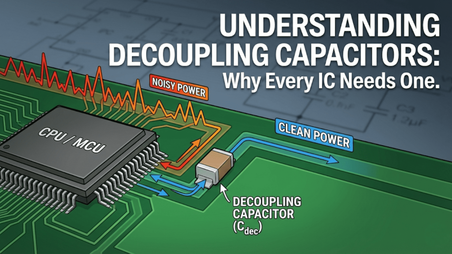
A decoupling capacitor is a small capacitor—typically 100nF ceramic—placed directly between an IC’s power supply pin (VCC/VDD) and its ground pin (GND), as close to the IC as possible. When the IC switches internally, it demands sudden bursts of current from the power supply. These current spikes travel through the inductance of the PCB traces and cause momentary voltage dips on the supply rail—which corrupt the IC’s logic and cause erratic behavior. The decoupling capacitor acts as a local energy reservoir sitting right next to the IC, supplying these instantaneous current demands from its stored charge before the power supply can respond, smoothing out the voltage and preventing supply-induced glitches.
Introduction: The Invisible Problem Causing Visible Chaos
You’ve carefully assembled a microcontroller circuit. Every connection is correct, the code is verified, the power supply measures exactly 3.3V. You power it up, and the circuit behaves erratically — random resets, spurious values from sensors, communication errors that come and go unpredictably. You check the wiring again. Nothing wrong. You reflash the firmware. Same behavior. You replace the microcontroller. Still the same.
The culprit is invisible on a multimeter and easy to miss on a schematic: missing or poorly placed decoupling capacitors.
Decoupling capacitors are among the least glamorous components in electronics. They don’t perform obviously useful work — they don’t amplify, filter in the conventional sense, store energy for long periods, or do anything you can easily see or measure with basic equipment. Yet they are absolutely essential. Every professional PCB designer adds them reflexively, without conscious thought, because their absence reliably causes problems and their presence reliably solves them.
For beginners and self-taught engineers, decoupling capacitors are often the last thing considered and the first thing responsible for mysterious circuit failures. This creates a frustrating gap: someone can understand digital logic, program microcontrollers, and design correct schematics but still have unreliable hardware because they don’t understand this one fundamental concept.
This article closes that gap completely. We’ll explore what decoupling capacitors actually do at the physics level, why integrated circuits create the problem they solve, how to choose the right values, where on the PCB they must be placed (placement matters enormously), what happens when you leave them out, and how to approach decoupling for different types of circuits — from simple microcontroller designs to high-speed digital systems.
The Problem: What Happens Inside an IC When It Switches
Digital Switching Creates Current Spikes
Modern digital ICs — microcontrollers, FPGAs, processors, logic gates — are built from CMOS transistors. Each CMOS gate consists of a P-channel and N-channel MOSFET pair. When a gate switches state (LOW to HIGH or HIGH to LOW), both transistors are momentarily conducting simultaneously during the transition — creating a brief but intense current spike from the power supply to ground.
The scale of the problem:
A simple logic gate might switch in a few nanoseconds and draw a spike of a few milliamps. But a microcontroller contains thousands of gates, and when executing code, many gates switch simultaneously. An AVR microcontroller running at 16MHz might have hundreds of gates switching every clock cycle. An FPGA might have tens of thousands of gates switching simultaneously.
The result: current demand from the IC’s power supply pin is not smooth and continuous — it’s a rapid series of spikes, each spike demanding tens or hundreds of milliamps for periods of nanoseconds to microseconds.
Power Supply Trace Inductance: The Enemy
Here is where the fundamental problem arises. Every wire, every PCB trace, every component lead has inductance. The inductance per unit length of a typical PCB trace is approximately 1–10 nanohenries per centimeter.
Why inductance matters at high frequencies:
Inductance resists changes in current. The voltage required to force a current change through an inductor is: V = L × dI/dt
When an IC demands a sudden current spike (high dI/dt), the inductance of the power supply trace creates a voltage drop proportional to how fast the current changes:
V_drop = L × (ΔI / Δt)
Worked example:
IC demands 100mA spike in 10 nanoseconds. Power supply trace inductance: 5nH (50mm of trace at 1nH/cm).
V_drop = 5nH × (100mA / 10ns) = 5 × 10⁻⁹ × 10⁷ = 0.05V = 50mV
A 50mV dip on a 3.3V supply might seem small, but:
- Noise margin for 3.3V CMOS logic is typically ±0.3V
- Multiple ICs switching simultaneously multiply this effect
- The power supply can’t respond fast enough (bandwidth of typical regulator: 100kHz–1MHz; nanosecond spikes are at GHz frequencies)
In a real system without decoupling, voltage dips of 100–500mV on supply rails are common, easily exceeding noise margins and causing logic errors.
The Power Supply Can’t Respond Fast Enough
Even if you have a perfect, ideal voltage regulator maintaining exactly 3.3V, it physically cannot respond to nanosecond-duration current spikes. Voltage regulators operate with feedback loops that have bandwidths of perhaps 100kHz to 1MHz — corresponding to response times of 1–10 microseconds. Nanosecond current spikes are 1,000 to 100,000 times faster than the regulator can react.
The regulator sees the average load, not the instantaneous spikes. From the regulator’s perspective, the supply voltage is fine. From the IC’s perspective, the local supply voltage is bouncing up and down with every switching event.
The Solution: What Decoupling Capacitors Do
The Local Energy Reservoir
A decoupling capacitor placed between VCC and GND right next to the IC acts as a local energy reservoir — a tiny, fast, local power supply that the IC can draw from immediately, without waiting for charge to travel from the main supply through the (inductance-limited) trace.
The mechanism:
- Between current spikes: The main power supply charges the decoupling capacitor through the supply trace. The capacitor charges to VCC.
- During a current spike: The IC demands current faster than the supply can provide through the inductance. The decoupling capacitor supplies this current from its stored charge. It begins discharging.
- After the spike: The voltage dip on the IC’s supply pin is small because the capacitor maintained the voltage. The supply trace now supplies current both to the IC and to recharge the capacitor. Eventually equilibrium is restored.
The key physics: the capacitor can supply current limited only by its own impedance (very low at high frequencies) and the short trace from capacitor to IC pin (very low inductance). The main supply trace inductance is bypassed by this local reservoir.
Capacitor Impedance and Frequency
A capacitor’s impedance is: Z_C = 1 / (2π × f × C)
At low frequencies, a capacitor is a near-open circuit (high impedance). At high frequencies, a capacitor becomes a near-short circuit (low impedance). This is exactly what we want: the decoupling capacitor should present low impedance to the high-frequency switching noise while being effectively invisible to the DC supply voltage.
Impedance of 100nF capacitor at different frequencies:
| Frequency | Z_C |
|---|---|
| 60 Hz | 26,500 Ω (effectively open) |
| 1 kHz | 1,590 Ω |
| 100 kHz | 15.9 Ω |
| 1 MHz | 1.59 Ω |
| 10 MHz | 0.16 Ω |
| 100 MHz | 0.016 Ω (near short circuit) |
At the frequencies of switching noise (1MHz–1GHz), a 100nF capacitor presents very low impedance — exactly what’s needed to supply current and maintain supply voltage.
Why “Decoupling” and “Bypass” Capacitors
These two terms are used nearly interchangeably in practice, but there’s a subtle conceptual distinction:
Decoupling: The capacitor decouples the IC’s switching noise from the power supply rail — preventing the IC’s current spikes from propagating to and affecting other ICs on the same supply rail.
Bypass: The capacitor bypasses high-frequency noise around the IC’s power pin to ground — providing a low-impedance path for high-frequency currents that bypasses the inductance of the power supply trace.
In practice, both terms describe the same component doing the same job. “Decoupling” is more common in digital circuit discussions; “bypass” in RF and analog contexts. For this article’s purposes, they are the same thing.
Choosing Decoupling Capacitor Values
The 100nF Rule: Your Universal Starting Point
For almost every digital IC in almost every circuit, placing a 100nF (0.1μF) ceramic capacitor between VCC and GND, as close as possible to the IC’s power pin, is the universal starting point. This value is chosen because:
- Sufficient capacitance: 100nF stores enough charge to supply typical IC switching currents during the brief switching events
- Good high-frequency response: Ceramic capacitors are inherently low-ESR (explained below), giving good performance into the hundreds of MHz
- Low self-resonance: 100nF with typical parasitic inductance self-resonates at useful frequencies
- Universal availability: 0.1μF MLCC (Multi-Layer Ceramic Capacitor) in 0402 or 0603 package is one of the most abundant components in electronics
The reflex habit of experienced designers: Before placing any IC in a PCB layout, the experienced designer places 100nF capacitors on every power pin. Not because they always calculate the exact value needed — because experience has proven this prevents problems.
Why Ceramic Capacitors, Not Electrolytics
Electrolytic capacitors (the cylindrical ones with the stripe marking the negative terminal) have much higher ESR (Equivalent Series Resistance) and ESL (Equivalent Series Inductance) than ceramic capacitors.
ESR and ESL in decoupling context:
Every real capacitor has:
- ESR: Resistance in series — limits how quickly current can flow out of the capacitor
- ESL: Inductance in series — caused by the lead length and internal structure
At high frequencies, ESL dominates capacitor impedance and causes it to rise — exactly opposite of what we want. A capacitor with high ESL becomes a poor high-frequency decoupling component.
Typical values:
- Electrolytic capacitor 100μF: ESL ≈ 10–20nH, ESR ≈ 0.1–5Ω
- Ceramic capacitor 100nF (0603): ESL ≈ 0.5–2nH, ESR ≈ 0.01–0.1Ω
At 100MHz, the impedance of an electrolytic capacitor may be dominated by its ESL (~10nH → 6.3Ω) rather than its capacitance (100μF → 0.0016Ω). The electrolytic provides almost no decoupling at this frequency.
The ceramic capacitor’s low ESL means it remains effective well into the hundreds of MHz.
Why then use electrolytics at all? For bulk capacitance (energy storage for lower-frequency variations), electrolytics provide large capacitance inexpensively. The combination of both types covers the full frequency range.
Self-Resonant Frequency (SRF) of Capacitors
Every real capacitor has a self-resonant frequency where the capacitive reactance and inductive reactance (ESL) cancel:
f_SRF = 1 / (2π × √(L_ESL × C))
Below SRF: capacitor behaves capacitively (good decoupling) At SRF: capacitor has minimum impedance (best decoupling at this frequency) Above SRF: capacitor behaves inductively (poor decoupling, gets worse with frequency)
Practical implication: Choose decoupling capacitor values so their SRF falls in the frequency range of the noise you’re suppressing.
Smaller capacitance + smaller package = lower ESL = higher SRF = effective at higher frequencies.
For a modern 1GHz microprocessor:
- 100nF 0603: SRF ≈ 50–100MHz — useful
- 100nF 0402: SRF ≈ 100–200MHz — better
- 10nF 0402: SRF ≈ 300–500MHz — better still at high frequency
- 1nF 0402: SRF ≈ 1GHz range — for highest frequency
Multiple Capacitor Values: The Two-Capacitor Strategy
Professional designs use two (or more) capacitor values per IC power supply:
1. Bulk capacitor (1μF–100μF): Handles lower-frequency variations (100kHz–10MHz range), provides charge reservoir for sustained load changes. Often ceramic 1μF–10μF for digital ICs; electrolytic 47μF–470μF for power supply outputs.
2. High-frequency bypass (10nF–100nF): Handles high-frequency spikes (10MHz–1GHz range). Always ceramic, small package.
Some designs add a third value (1nF or 100pF) for very high-frequency (>500MHz) suppression.
Why the combination works: Each capacitor handles a different frequency range. The bulk capacitor, with its larger capacitance, fills in when the bypass runs dry over longer current demands. The bypass capacitor, with its lower ESL, responds faster to brief high-frequency spikes.
Together they maintain low supply impedance across a much wider frequency range than either alone.
Specific Value Guidelines by Application
Simple AVR/Arduino microcontroller (16MHz):
- 100nF ceramic per VCC pin (usually 2 pins on AVR)
- Optional: 10μF electrolytic near the power connector
- Total: 2–3 capacitors, all cheap and tiny
ARM Cortex-M MCU (48–168MHz, STM32, nRF52):
- 100nF ceramic per VCC pin
- 1μF ceramic near each VCC pin (or one shared for closely spaced pins)
- Total: 4–10 capacitors
FPGA (running at 100MHz–500MHz+):
- Multiple 100nF per supply bank
- Multiple 1μF per supply bank
- Possibly 10nF for each high-speed I/O power supply pin
- Total: Dozens of capacitors
Op-amp (signal path, ±15V dual supply):
- 100nF per supply rail (positive and negative)
- 10μF electrolytic per supply rail (for low-frequency supply stabilization)
- Total: 4 capacitors per op-amp supply (2 ceramic + 2 electrolytic)
74HC logic series (5V or 3.3V):
- One 100nF ceramic per IC (or per power pin if multiple VCC pins)
- One 10μF–100μF bulk electrolytic per PCB power rail
Placement: The Most Critical Factor
Why Placement Matters More Than Value
You can choose the right capacitor value but place it 5cm away from the IC and get almost no benefit. You can choose a slightly suboptimal value but place it 2mm from the IC pin and get excellent decoupling.
The reason: Every millimeter of PCB trace between the decoupling capacitor and the IC power pin adds inductance. That inductance reduces the effectiveness of the capacitor for high-frequency signals — exactly canceling the benefit we’re trying to achieve.
A trace from capacitor to IC power pin that’s 1cm long adds approximately 5–10nH of inductance. At 100MHz: X_L = 2π × 100MHz × 10nH = 6.3Ω
That 6.3Ω in series with the capacitor means the capacitor can only supply current through a 6.3Ω series impedance — largely defeating the decoupling purpose.
The Golden Rule: As Close as Possible
Place decoupling capacitors as close as physically possible to the IC’s power pin, with the shortest possible traces from capacitor pad to IC pad.
In practice:
- On a PCB: The capacitor pad should be within 1–2mm of the IC power pin pad
- The trace from capacitor to power pin: As short and wide as possible
- The trace from capacitor to ground: As short as possible to the nearest ground plane or ground via
Layout priority:
- Capacitor placed immediately adjacent to IC VCC pin
- Direct trace from capacitor to VCC pin (no other components in this trace)
- Direct via or trace from capacitor ground to power plane or nearby ground pour
- Then, longer trace from main power supply to capacitor VCC pad
The goal is to minimize the inductance of the loop: VCC pad → capacitor → GND pad → IC GND pin → IC internal switching → IC VCC pin → back to capacitor. Smaller loop = less inductance = better decoupling.
PCB Layout Strategy
For a DIP or through-hole IC: Place 100nF capacitor immediately beneath the IC between pins 14 (VCC) and 7 (GND) for a 14-pin DIP, for example. Route as short as possible.
For a SOIC or QFP SMD IC:
- Place 100nF 0402 or 0603 capacitors immediately adjacent to each VCC/GND pin pair
- On a 2-layer board: Capacitor on same side as IC, connected through very short traces, ground pad connected via through-hole to ground on bottom layer
- On a 4-layer board with power plane: Capacitor VCC pad connected to VCC plane through short trace; capacitor GND pad connected directly to GND plane through via
For BGA devices (processors, FPGAs): The ideal placement is directly underneath the BGA on the back side of the board, with vias through the PCB connecting to the power balls. This minimizes the current loop area. High-density BGA designs may require micro-vias (blind/buried vias) for capacitor placement in the via field beneath the device.
Via Placement
In multilayer designs, the via from the decoupling capacitor to the ground plane is itself a source of inductance. Each via adds approximately 0.5–1nH.
Best practice:
- Place ground vias as close as possible to the capacitor ground pad
- For high-frequency designs, use two vias from each capacitor ground pad to halve the via inductance
- Keep both supply and ground vias close to the IC
What Happens Without Decoupling Capacitors
Real Failure Modes
Designers who omit or misplace decoupling capacitors encounter characteristic failure patterns:
Random resets: Voltage dips during heavy switching activity cause the supply to briefly dip below the microcontroller’s brownout reset threshold, triggering a reset without any apparent cause. The reset may occur only during certain operations (writing to flash memory, running certain algorithms) because those operations cause the most simultaneous switching.
Communication errors: I²C, SPI, and UART communications fail intermittently. The switching activity of the communication peripheral creates supply noise that corrupts the very data being transmitted. Errors are often worse when the MCU is simultaneously doing other work.
ADC inaccuracy: Analog-to-digital conversions give wrong results, often varying even when the input is stable. The ADC reference voltage and supply are contaminated by digital switching noise, corrupting the conversion result. This is particularly common when ADC conversions happen during or immediately after switching activity.
Oscillator instability: Crystal oscillators or RC oscillators become frequency-unstable when the supply voltage varies. The microcontroller’s timing becomes unreliable, causing communication baud rate errors and timing-dependent failures.
Logic glitches: Individual logic gates receive corrupted supply voltage during switching, causing them to briefly produce incorrect outputs. In complex digital systems, these glitches can propagate through multiple logic levels, causing unpredictable behavior.
EMI failures: The noise currents generated by IC switching and reflected back onto the power supply radiate from power supply traces and wires. Without decoupling, circuits that pass regulatory EMC (electromagnetic compatibility) testing with proper decoupling may fail without it.
The Difficult Diagnosis
The most frustrating aspect of decoupling problems is that they’re difficult to diagnose without the right equipment. A standard multimeter measuring supply voltage shows a stable 3.3V — it simply cannot respond fast enough to see nanosecond spikes. Even a basic oscilloscope set to DC coupling shows a flat supply voltage — the probe’s input capacitance and the oscilloscope’s bandwidth determine what’s visible.
To see decoupling-related noise:
- Use an oscilloscope with adequate bandwidth (200MHz+ for most microcontroller work)
- Use a short, direct probe with no lead — press the probe tip directly to the IC power pin and use the ground spring (not a ground lead) connected to the nearest ground pad
- Set the oscilloscope to AC coupling and 50–100mV/division
- Run the firmware doing maximum switching work
Only then do the supply voltage bounces become visible — and often they’re surprising in magnitude.
Special Cases and Advanced Considerations
Ferrite Beads as Part of the Decoupling Strategy
For sensitive analog circuits (precision ADC references, audio, low-noise sensors) sharing a supply with noisy digital circuits, a ferrite bead in series with the analog supply provides additional filtering:
Digital supply rail
      │
   [Ferrite bead]    ← High impedance to high-frequency noise
      │
   Analog supply rail ──[100nF]──[10μF]── GND
      │
Analog ICsThe ferrite bead is a high-frequency inductor that, combined with the decoupling capacitors, forms a low-pass filter for the analog supply. Digital switching noise is blocked; the stable DC supply passes through.
Selecting ferrite beads: Choose a ferrite bead rated for the maximum current required by the analog section, with impedance at least 100Ω at the problematic frequency (typically 100MHz).
Decoupling for Analog ICs
Op-amps and other analog ICs need decoupling too, but the emphasis shifts:
- Lower frequencies matter more (audio bandwidth: 20Hz–20kHz; precision measurement DC to kHz)
- Power supply rejection ratio (PSRR) of the op-amp attenuates supply noise somewhat, but finite PSRR means some noise still appears at the output
- Both supply rails (positive and negative for dual-supply op-amps) need decoupling
- Typical: 100nF ceramic + 10μF electrolytic per supply rail, placed close to the IC
Decoupling on Breadboards
Here’s an uncomfortable truth: breadboards are terrible for high-frequency decoupling.
The breadboard’s contact rails and jumper wires have substantial inductance — easily 10–50nH per connection. Even with 100nF capacitors placed at the IC’s VCC/GND pins, the breadboard parasitic inductance largely negates their effectiveness above a few MHz.
This is why:
- Circuits that work perfectly on a PCB with proper decoupling may be unreliable on breadboard
- High-speed microcontrollers (ARM Cortex-M at 168MHz) may behave erratically on breadboard even with decoupling capacitors
- Older, slower microcontrollers (8MHz AVR) are more breadboard-tolerant
- A PCB, even a simple one, provides dramatically better decoupling effectiveness
For breadboard prototyping, place 100nF capacitors as close to the IC as possible and accept that high-frequency performance will be compromised.
Comparison Table: Decoupling Capacitor Options
| Type | Value | ESR | ESL | SRF | Best For | Avoid When |
|---|---|---|---|---|---|---|
| Ceramic 100nF 0402 | 100nF | ~10mΩ | ~0.4nH | ~200MHz | High-speed digital, MCUs, FPGAs | High current bulk storage |
| Ceramic 100nF 0603 | 100nF | ~20mΩ | ~0.7nH | ~100–150MHz | General digital ICs, easy hand-solder | Very high-speed (>500MHz) |
| Ceramic 1μF 0603 | 1μF | ~25mΩ | ~0.7nH | ~60MHz | Medium-bulk + HF bypass combo | High voltage (degrades vs. rated voltage) |
| Ceramic 10μF 0805 | 10μF | ~50mΩ | ~1nH | ~20MHz | Near-IC bulk capacitance | High voltage, high-precision analog |
| Electrolytic 47μF radial | 47μF | ~0.1–1Ω | ~10–20nH | ~1–5MHz | Power supply output bulk, low-freq | High-frequency decoupling (useless >10MHz) |
| Electrolytic 470μF radial | 470μF | ~0.05–0.5Ω | ~15–30nH | ~0.5MHz | Large bulk reservoir at supply input | Anything high-frequency |
| Tantalum 10μF | 10μF | ~0.1–0.3Ω | ~5–10nH | ~5MHz | Compact bulk, space-constrained | Reverse voltage (explodes), high surge |
| Ceramic 1nF 0402 | 1nF | ~5mΩ | ~0.3nH | ~1–3GHz | RF decoupling, very-high-speed digital | General purpose (too small alone) |
Practical Checklist: Decoupling Done Right
Before finalizing any PCB design or verifying a working breadboard circuit, run through this checklist:
Component selection: ☐ Used ceramic (MLCC) capacitors for high-frequency bypass — not electrolytics ☐ Chosen 100nF as minimum value for each IC VCC pin ☐ Added 1μF–10μF ceramic for bulk decoupling per IC or per power supply section ☐ Verified capacitor voltage rating exceeds supply voltage (100nF 10V capacitor on 5V supply is fine; 100nF 6.3V capacitor on 5V supply has reduced actual capacitance due to DC bias voltage derating)
Placement: ☐ Every IC has at least one decoupling capacitor within 2–3mm of its VCC pin ☐ Capacitors placed before the main power trace reaches the IC (capacitor between trace and IC pin, not after the IC) ☐ Ground side of capacitor connected to nearest ground pour/plane with short via or trace — not through a long route
Multiple power pins: ☐ ICs with multiple VCC pins (common in FPGAs, ARM processors) have capacitor on each VCC pin ☐ MCUs with separate analog VCC (AVCC, AVDD) have separate decoupling — do not rely on digital VCC decoupling capacitor
Sensitive circuits: ☐ Analog sections have ferrite bead separation from digital power ☐ ADC reference voltage (VREF) decoupled separately from VCC — typically 100nF right at VREF pin
Conclusion: The Habit That Prevents Hundreds of Problems
Decoupling capacitors represent one of those concepts that, once truly understood, become automatic. Every time you see an IC in a circuit, you think “power pin, decoupling cap, close as possible.” You don’t agonize over whether to add them — you add them reflexively, the way a carpenter uses a level without consciously deciding whether it’s necessary.
The Core Principles
Current spikes, not voltage — the underlying problem. ICs don’t draw constant current from the supply; they draw rapid, intermittent spikes. These spikes, multiplied by the inductance of supply traces, create supply voltage noise that corrupts digital logic.
Local reservoir, not cable from the main supply. The decoupling capacitor is a tiny local supply sitting right next to the IC, ready to deliver current at nanosecond speed. The main supply provides the average current; the capacitor handles the peaks.
Placement beats value. A correctly sized capacitor placed 5cm away is worse than a slightly undersized capacitor placed 2mm away. Minimize the current loop from supply → cap → IC power pin → IC GND pin → cap ground → supply.
Ceramic, not electrolytic, for high-frequency bypass. Ceramic capacitors have low ESR and ESL, remaining effective well into the hundreds of MHz. Electrolytics are for bulk storage at lower frequencies.
Multiple values cover multiple frequencies. 100nF handles high-frequency spikes; 1μF–10μF handles medium-frequency bulk demand; 47μF–470μF at the supply output handles sustained load variations.
What This Knowledge Enables
With proper decoupling in your designs, circuits behave predictably and reliably. ADC readings are accurate. Communication is error-free. Microcontrollers don’t reset unexpectedly. The gap between “works on breadboard sometimes” and “works on PCB always” often reduces to proper decoupling.
More broadly, understanding decoupling builds the physical intuition for high-frequency circuit behavior that separates circuit builders from circuit designers. The inductance of traces, the frequency-dependent behavior of components, the importance of current loop area — these concepts, learned through understanding decoupling capacitors, apply to signal integrity, EMC, and RF design throughout your engineering practice.
A 100nF capacitor costs less than a cent. The circuit reliability it provides is worth far more.