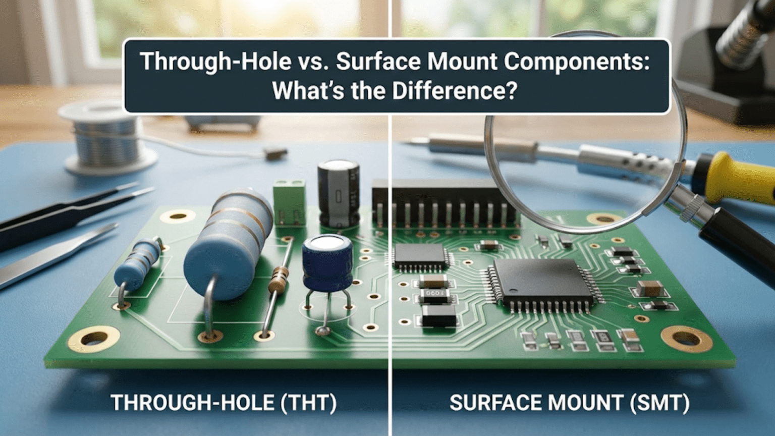
Through-hole components have long wire leads that insert through drilled holes in a PCB and are soldered on the opposite side, while surface mount components (SMD/SMT) have small flat or stubby terminals that solder directly onto pads on the PCB surface with no holes required. Through-hole components are larger, easier to hand-solder, and mechanically stronger, making them ideal for connectors, high-power parts, and beginners. Surface mount components are dramatically smaller, cheaper to manufacture at volume, and dominate modern commercial electronics because they can be placed automatically at high speed and mounted on both sides of a PCB for maximum density.
Introduction: Two Technologies, One Purpose
Open any modern smartphone and you’ll find a PCB densely packed with hundreds of tiny, almost microscopic components soldered flat to the board’s surface—no holes, no protruding wires, just minuscule packages bonded directly to copper pads. Open a vintage radio from the 1970s and you’ll find components with long wire leads threaded through the board, soldered beneath. Open a hobbyist Arduino kit and you’ll find both technologies coexisting.
These are the two dominant component mounting technologies in electronics: through-hole (TH) and surface mount (SMD/SMT). Each emerged from different eras, serves different needs, and offers a distinct set of trade-offs. Understanding the difference between them—not just superficially, but in terms of the physical, electrical, and manufacturing implications—is fundamental knowledge for anyone working with electronics.
The through-hole versus surface mount distinction affects everything: how you solder, what tools you need, how small your circuit can be, how much components cost in quantity, how reliable the assembly is under mechanical stress, and whether you can repair or modify the board yourself. Choosing the wrong technology for a given application creates problems; choosing the right one makes assembly easier and the end product better.
For beginners, this topic often carries an unspoken anxiety. Surface mount components look impossibly small and fragile—surely only professionals with expensive equipment can work with them? In reality, the situation is more nuanced. Yes, the smallest SMD packages require specialized tools and techniques. But many SMD packages are quite manageable with standard hand-soldering tools, and the fundamentals of hand-soldering through-hole and hand-soldering SMD are more similar than different.
This comprehensive guide examines through-hole and surface mount technologies in depth. We’ll explore the physical construction of both types, understand how they’re manufactured and assembled, compare their electrical and mechanical characteristics, survey the component types available in each format, and develop clear guidance for when to use each technology—including the important hybrid approach where both coexist on the same board.
Through-Hole Components: The Traditional Standard
What Through-Hole Means Physically
A through-hole component has one or more leads (wire legs) that extend from the component body. These leads are inserted through precisely drilled holes in the PCB—one lead per hole—passing completely through the board thickness. On the opposite side, the leads are soldered to the copper pads that surround each hole, and the excess lead length is trimmed flush.
The hole, combined with the plated copper barrel inside it and the pad on the solder side, forms the mechanical and electrical connection. The solder fills the gap between the lead and the hole barrel, creating both a physical bond and an electrical connection.
Why this works so well mechanically: The lead passes through the board, and solder fills the annular space between lead and plated barrel. This creates a connection that resists forces from multiple directions—pull the component upward and the solder joint resists; push it sideways and the barrel in the board resists. Through-hole components are essentially anchored to the PCB. This robustness is why connectors, high-current terminals, and components subject to mechanical stress almost always use through-hole mounting even on otherwise all-SMD boards.
Anatomy of a Through-Hole PCB Pad
Drill hole: Precisely sized to accept the component lead. Standard drill sizes are 0.8mm, 1.0mm, 1.2mm, 1.6mm for most through-hole components.
Annular ring: The copper pad surrounding the hole on the top and bottom surfaces. Width of annular ring matters—too narrow and a slightly off-center drill breaks the connection to the trace.
Plated through-hole (PTH): The inside of the drilled hole is coated with copper, creating electrical connection between top and bottom copper rings and allowing current to flow through the via-like structure.
Unplated through-hole (UPTH): Holes for mechanical mounting only (mounting screws, panel connectors) with no copper plating.
Common Through-Hole Package Types
Axial lead: Component body is cylindrical or rectangular with one lead exiting each end in line with the body axis. The component mounts horizontally flat on the board or stands vertically with one lead bent 180°.
Examples: Carbon and metal film resistors, small-value ceramic capacitors, small diodes (1N4148, 1N4007), some inductors.
Radial lead: Both leads exit from the same side (bottom) of the component, enabling vertical mounting that saves PCB real estate.
Examples: Electrolytic capacitors (the most common radial component), some inductors, buzzers.
DIP (Dual Inline Package): Rectangular IC package with two parallel rows of leads, typically 2.54mm (0.1 inch) pitch. The most common through-hole IC package.
DIP-8 (8 pins): Small op-amps, EEPROMs DIP-14, DIP-16: Logic gates, simple microcontrollers DIP-28, DIP-40: Larger microcontrollers (ATmega328P in DIP-28)
DIP packages fit perfectly in breadboards (0.1″ pitch matches breadboard spacing), which is why they remain popular for prototyping even as surface mount dominates production.
SIP (Single Inline Package): Single row of leads. Used for resistor networks, some modules, SIP capacitor arrays.
TO (Transistor Outline) packages: Various metal can and plastic packages for discrete transistors, voltage regulators, and power devices.
- TO-92: Small plastic package, 3 leads, common for small signal transistors (2N2222, BC547)
- TO-220: Larger plastic package with tab for heat sinking, used for power transistors, voltage regulators (7805, IRF540)
- TO-247: Larger still, for higher power devices
- TO-3: Metal can package for high-power devices
Special purpose:
- Crystal holders (HC-49, HC-18): Quartz crystals in metal cases
- LED through-hole: 3mm, 5mm cylindrical LEDs with 2-pin axial leads
- Push buttons and tactile switches: 4-pin DIP mounting
- Large connectors: DB9, DB25, USB type A/B, audio jacks
Through-Hole Manufacturing: Wave Soldering
At production scale, through-hole components are assembled using wave soldering:
- Components are inserted into holes (by hand or automated insertion machine)
- Leads may be clinched (bent to hold components during handling)
- PCB passes over a wave of molten solder
- Solder wicks up into the plated holes by capillary action
- Leads are trimmed (often automatically)
Wave soldering efficiently solders all through-hole joints simultaneously—an entire board in seconds. However, it requires components to be on one side only (the component side), and the board must be masked to prevent solder from contaminating SMD components already on the solder side.
Hand Soldering Through-Hole Components
Through-hole components are significantly more accessible for hand soldering than surface mount because:
- Component leads are large enough to grip and manipulate manually
- PCB holes act as guides, keeping leads positioned while soldering
- Pads are large relative to the iron tip
- Standard 0.6–0.8mm solder wire works well
- The result (a small solder cone visible from both sides) is easy to inspect visually
This accessibility makes through-hole ideal for beginners, repair work, prototyping, and any application where hand assembly is preferred.
Surface Mount Components: The Modern Standard
What Surface Mount Means Physically
Surface mount components (SMDs — Surface Mount Devices) have no through-hole leads. Instead, they have:
- Flat pads (for chip components like resistors and capacitors)
- Gull-wing leads (short leads that curve outward and down, like a seagull’s wing)
- J-leads (leads that curve under the package body)
- BGA balls (Ball Grid Array — an array of solder balls on the package bottom)
- LCC/QFN lands (flat pads on the package edge or bottom)
These terminals rest directly on the PCB surface copper pads. Solder paste (a mixture of fine solder powder and flux) is applied to the pads, the component is placed on top, and the assembly passes through a reflow oven where the solder paste melts and solidifies to form joints.
Why this approach dominates modern electronics:
The elimination of holes allows:
- Much smaller components (no space wasted on lead length or hole diameter)
- Components on both sides of the PCB (no leads poking through to block the other side)
- Automated pick-and-place assembly at thousands of components per hour
- Smaller, lighter PCBs for a given circuit complexity
- Lower cost at volume (less PCB real estate, faster assembly)
SMD Package Size Codes
Passive SMD components (resistors, capacitors, inductors) use standardized size codes based on imperial dimensions in hundredths of an inch:
Imperial size codes:
| Code | Length × Width | Metric equivalent | Typical current use |
|---|---|---|---|
| 0201 | 0.020″ × 0.010″ | 0.5mm × 0.25mm | Advanced mobile, dense boards |
| 0402 | 0.040″ × 0.020″ | 1.0mm × 0.5mm | Modern commercial electronics |
| 0603 | 0.060″ × 0.030″ | 1.6mm × 0.8mm | Versatile; manageable by skilled hand-solderers |
| 0805 | 0.080″ × 0.050″ | 2.0mm × 1.25mm | Good for hobbyist hand-soldering |
| 1206 | 0.120″ × 0.060″ | 3.2mm × 1.6mm | Easy hand-soldering; higher power |
| 1210 | 0.120″ × 0.100″ | 3.2mm × 2.5mm | High capacitance, power applications |
| 2512 | 0.250″ × 0.120″ | 6.4mm × 3.2mm | High-power resistors (1–2W) |
Metric size codes (increasingly common): The metric size code is approximately 10× the metric dimensions: a 0402 imperial = 1005 metric; 0603 imperial = 1608 metric.
For hobbyists:
- 0402: Very difficult by hand, requires practice and good magnification
- 0603: Achievable with good technique and magnification
- 0805 and larger: Comfortable for most hand-solderers
- 1206 and larger: Easy hand-soldering
SMD IC Packages
SOIC (Small Outline Integrated Circuit): Gull-wing leads on both long sides. 1.27mm pitch (0.05″). The most common SMD IC package for through-hole replacement. Significantly smaller than DIP but still relatively hand-solderable.
SOIC-8, SOIC-14, SOIC-16: Common sizes for op-amps, logic ICs, regulators
SSOP, TSSOP (Thin Shrink Small Outline Package): Narrower and thinner than SOIC. 0.65mm or 0.5mm pitch. Requires good technique for hand soldering.
QFP (Quad Flat Package): Gull-wing leads on all four sides. Pitches from 1.0mm down to 0.4mm for fine-pitch versions. Larger QFPs (0.8mm pitch, 32–100 pins) are achievable for experienced hand solderers; fine-pitch QFPs (0.4–0.5mm) require excellent technique or hot-air rework.
QFN (Quad Flat No-lead): Flat pads on the bottom edges of the package, no protruding leads. Often has a large exposed thermal pad underneath. Requires reflow oven for reliable soldering—the thermal pad makes hand soldering difficult. Very compact, excellent thermal performance.
BGA (Ball Grid Array): Grid of solder balls on the bottom of the package. Cannot be hand-soldered—requires reflow oven and typically X-ray inspection to verify joints. Used for processors, memory, and high-pin-count devices.
SOT (Small Outline Transistor) packages:
- SOT-23: 3-lead (transistors, small regulators, diodes), 1.9mm × 1.3mm
- SOT-23-5/6: 5 or 6 leads, small ICs
- SOT-223: Larger package with tab, for medium-power regulators
SOD (Small Outline Diode): SOD-123, SOD-323, SOD-523: Various sizes for SMD diodes
Surface Mount Manufacturing: Reflow Soldering
SMD assembly at production scale uses reflow soldering:
1. Solder paste printing: A stencil (thin metal sheet with apertures matching pad locations) is aligned over the PCB. Solder paste is squeegeed across the stencil, depositing precise volumes of paste on each pad.
2. Pick-and-place: Automated machines pick components from tape-and-reel feeders at rates of 10,000–100,000+ components per hour and place them on the solder paste with ±25μm accuracy. The paste’s stickiness holds components in place.
3. Reflow oven: The PCB passes through a conveyor oven with precisely controlled temperature zones:
- Preheat zone: Gradually raises PCB to ~150°C, activating flux
- Soak zone: Holds temperature for flux activation and temperature equalization
- Reflow zone: Raises to 230–250°C (for SAC305), melting solder paste and forming joints
- Cooling zone: Controlled cooling prevents thermal shock
4. Inspection: Automated Optical Inspection (AOI) cameras examine every joint for defects. X-ray inspection verifies BGA joints. Manual inspection for complex or critical areas.
Double-sided assembly: SMD components can mount on both sides of a PCB. The first side is reflowed, the board is flipped, components placed on the second side, and a second reflow pass solders them. Gravity is managed—components on the already-soldered side don’t fall off during second reflow because surface tension of molten solder holds them.
Hand Soldering SMD Components
Despite the dominance of automated assembly, SMD components can be hand-soldered effectively:
For chip components (0402–1206):
- Tin one pad with a small amount of solder
- Hold component with tweezers, touch to pad
- Apply iron briefly—component self-aligns as solder wets both pad and component terminal
- Solder the second pad with solder wire
- Touch up first pad for ideal joint shape
For IC packages (SOIC, TSSOP):
- Tin one corner pad
- Align IC, reflow corner pin to tack in place
- Solder opposite corner pin, checking alignment
- Solder remaining pins with iron + solder wire
- For fine-pitch: Use flux + drag soldering technique (wipe iron loaded with solder across all pins; bridges form then wick back with capillary action and added wick)
Essential tools for SMD hand soldering:
- Fine chisel or bevel tip (0.5–1.0mm)
- Fine solder wire (0.3–0.5mm)
- Good magnification (at least 3–5×, ideally 10–20×)
- Flux pen or gel flux
- Brass-tip tweezers (non-magnetic)
- Desoldering wick (fine braid)
Key Differences: Head-to-Head Comparison
Physical Size
Through-hole: Smallest practical through-hole components (0.25W resistors) are approximately 6mm long × 2mm diameter. DIP-8 ICs occupy about 10mm × 7mm of board space with two rows of pins.
Surface mount: An 0402 resistor is 1mm × 0.5mm — about 1/25th the area of a 0.25W through-hole resistor. A SOIC-8 IC occupies approximately 5mm × 4mm compared to DIP-8’s 10mm × 7mm footprint.
Impact: At equivalent circuit complexity, SMD boards can be 3–10× smaller than through-hole equivalents. Modern smartphones would be literally impossible to build with through-hole components.
Mechanical Strength
Through-hole: The lead running through the board and soldered on both sides creates a joint with excellent resistance to pulling forces (perpendicular to board) and lateral stress. Particularly important for connectors, switches, and components subject to mechanical force during use.
Surface mount: Solder joint is purely on the surface. Under direct pulling force, SMD joints fail more easily than through-hole equivalents. However, properly designed SMD joints on a properly designed PCB are very reliable—the mechanical stress distribution matters enormously.
Practical implications: Connectors (USB, audio jacks, power connectors) where plugging/unplugging exerts force are often through-hole or use mechanical retention features even on SMD boards. Components that users directly interact with (buttons, potentiometers) benefit from through-hole mounting for mechanical durability.
Thermal Characteristics
Through-hole: Lead length provides a thermal path that slows heat transfer from iron to component body during soldering—a safety advantage for heat-sensitive components. Also means more physical separation between heat-generating components and the PCB.
Surface mount: Components mount directly on the PCB surface with minimal thermal distance from the board. This means:
- Better thermal coupling between component and PCB (often beneficial for cooling)
- Lower thermal resistance to board (good for power devices with thermal pads)
- Heat-sensitive components (certain crystals, some LEDs) can be damaged more easily if not careful during hand soldering
Electrical Performance
Through-hole: Lead inductance (the inductance of the long component leads) becomes significant at high frequencies (>100MHz). Long leads also create small loop areas that can radiate or pick up electromagnetic interference.
Surface mount: Short, stubby terminals have negligible lead inductance. SMD components perform significantly better than through-hole at RF and high-speed digital frequencies. This is a major reason why virtually all RF, microwave, and high-speed digital circuits use SMD exclusively—the electrical performance at high frequencies is genuinely superior.
Parasitic capacitance: SMD packages also have lower parasitic capacitance than through-hole packages, further improving high-frequency performance.
Assembly
Through-hole assembly:
- Manual insertion: Slow but accessible to anyone
- Automated insertion: Possible but slower than SMD pick-and-place
- Wave soldering: Fast, reliable, but requires all components on one side
- Hand soldering: Accessible with basic equipment
Surface mount assembly:
- Manual placement: Feasible for larger packages with tweezers and patience
- Automated pick-and-place: Extremely fast (thousands per hour), highly accurate
- Reflow soldering: Consistent, reproducible, scalable
- Hand soldering: Possible for most packages with good technique and tools
Reworkability and Repair
Through-hole:
- Easier to desolder by hand
- Components can be extracted with desoldering pump or wick
- Replacement is straightforward
- More forgiving of technique errors
Surface mount:
- Chip components: Reasonably easy to remove and replace with hot air or iron
- SOIC/SSOP ICs: Manageable with hot air and flux
- QFN/BGA: Requires hot air station, proper temperatures, possible reballing
- Very fine-pitch or BGA: Practical repair only with professional rework station
For field repair and hobbyist rework, through-hole is significantly more accessible. For production rework, both have established techniques.
Cost
Components: Passive SMD components (0402, 0603 resistors and capacitors) in volume are often cheaper than equivalent through-hole parts because they’re produced in enormous quantities and the material volume is smaller.
Through-hole ICs (DIP packages) often cost more than equivalent SOIC packages because the DIP package is a legacy format produced in smaller quantities.
Assembly: At volume, SMD assembly is dramatically cheaper than through-hole:
- Pick-and-place speed: SMD 5–10× faster than through-hole insertion
- No lead trimming required
- Solder paste is consistent volume; hand solder is not
- Double-sided placement increases density without doubling assembly cost
Through-hole assembly has a cost floor below which it cannot go regardless of volume; SMD assembly cost drops with scale.
PCB cost: SMD boards are smaller for equivalent complexity, directly reducing PCB cost. No through-holes means simpler drill requirements.
Hybrid Assemblies: The Best of Both Worlds
Modern PCBs rarely use exclusively one technology. Most real-world boards are hybrids, deliberately using through-hole for specific components where it excels and SMD for everything else.
Why Hybrids Make Sense
Through-hole where mechanical strength matters:
- USB connectors: Heavy use, mechanical stress from plug/unplug → through-hole
- Power connectors (barrel jacks, terminal blocks): High current and mechanical force → through-hole
- Audio jacks: User interaction, physical force → through-hole
- Mounting hardware: Standoffs, screws → unplated through-holes
Through-hole where high power is needed:
- Large electrolytic capacitors (>1000μF): Larger through-hole parts available, easier thermal management
- Power MOSFETs and transistors in TO-220: Through-hole with heatsink capability
- High-power resistors (5W+): Through-hole wirewound types
- Inductors for power conversion: Through-hole for high current ratings
Through-hole where user adjustability matters:
- Trim potentiometers: Adjustment requires accessibility
- DIP switches: Manual configuration during development
- Socketed components: Easy replacement during development or maintenance
SMD for everything else:
- All signal-level passives (resistors, capacitors, inductors)
- Signal ICs (op-amps, comparators, logic)
- Microcontrollers, FPGAs (TQFP, QFN packages)
- LEDs for indicators (SMD LEDs mount flat, have better light distribution)
- Decoupling capacitors (must be physically close to ICs)
Manufacturing Considerations for Hybrid Boards
Hybrid boards add manufacturing complexity:
- Through-hole components usually wave-soldered after SMD reflow
- SMD on solder side must be masked during wave soldering
- Some SMD near through-hole components may be damaged by wave solder temperatures
- Hand assembly often combines phases: SMD reflow first, then hand solder through-hole
For low-volume production, through-hole components on a primarily SMD board are often hand-soldered after the automated SMD reflow step.
Comparison Table: Through-Hole vs. Surface Mount
| Characteristic | Through-Hole (THT) | Surface Mount (SMD/SMT) |
|---|---|---|
| Lead style | Long wire leads through PCB holes | Short flat terminals or pads on PCB surface |
| Smallest passive size | ~6mm × 2mm (0.25W resistor) | 0.5mm × 0.25mm (0201 resistor) |
| PCB holes required | Yes — drilled, copper-plated | No — traces and pads only |
| Both PCB sides usable | No — leads block reverse side | Yes — components on both sides |
| Mechanical strength | Excellent — lead anchors through board | Good — surface bond only |
| High-frequency performance | Limited — lead inductance significant | Excellent — minimal parasitics |
| Hand soldering difficulty | Easy to moderate | Moderate to difficult (size-dependent) |
| Automated assembly speed | Slow (insertion + wave solder) | Very fast (pick-and-place + reflow) |
| Volume cost | Higher (labor, PCB area) | Lower (speed, density) |
| Repairability | Easy | Moderate to difficult (package-dependent) |
| Breadboard compatible | Yes (0.1″ pitch DIP) | No |
| Prototyping friendliness | Excellent | Moderate |
| Component availability | Good, full range | Excellent, largest selection |
| Power handling (per unit) | Good — large packages available | Improving — larger packages available |
| Typical applications | Connectors, power, hobbyist, repair | Commercial electronics, high density, RF |
Practical Guidance: Which to Choose?
For Absolute Beginners
Start with through-hole. This is not a suggestion to avoid surface mount forever—it’s a recognition that through-hole builds the physical intuition that makes SMD accessible later.
Through-hole teaches:
- How components physically look and how to identify them
- Soldering fundamentals without the additional challenge of tiny size
- Circuit debugging at a scale where measurement probes fit easily
- The satisfaction of building functional circuits without equipment barriers
Arduino starter kits, breadboard experiments, and through-hole PCB kits are the right starting point. Invest 3–6 months here before advancing.
For Developing Hobbyists
Learn 0805 SMD as the next step. At 2mm × 1.25mm, 0805 components are small enough to appreciate the SMD form factor without being torturously difficult.
A dedicated 0805 SMD soldering practice kit (available inexpensively from multiple vendors) teaches:
- Tweezers technique
- Flux use and how it transforms SMD soldering
- IC hand-soldering with SOIC packages
The jump from 0805 to 0603 is modest; from 0603 to 0402 requires better magnification and more patience.
For Designing Original PCBs
Design primarily in SMD with through-hole exceptions. This matches professional practice and delivers real advantages:
- Smaller, cheaper PCBs
- Components readily available in SMD (enormous selection)
- Better electrical performance
- Cheaper at any quantity above ~50 units
Use through-hole for: all connectors, any component subject to mechanical stress, high-current/power devices, anything you might need to adjust or replace during development.
For Repair and Modification
Match what’s already on the board. Replacing a failed SMD component with a through-hole part is rarely practical (wrong pad layout, wrong physical size). Use the same technology as the original design, using appropriate tools for the package type.
Conclusion: Two Technologies, One Electronics Ecosystem
Through-hole and surface mount technologies are not competitors fighting for supremacy—they are complementary tools, each optimized for different parts of the electronics ecosystem. Through-hole’s mechanical strength, accessibility, and breadboard compatibility make it irreplaceable for connectors, power components, prototyping, and education. Surface mount’s miniaturization, electrical performance, and manufacturing efficiency make it the foundation of every commercial electronic product.
The Direction of the Industry
Surface mount technology has been steadily displacing through-hole in all applications where mechanical force isn’t a primary concern. Component packages continue shrinking—0201 and even 01005 are now standard in high-density designs. Many components are now available only in surface mount packages; trying to find a through-hole version is sometimes impossible.
For anyone serious about modern electronics, surface mount is not optional knowledge—it’s the lingua franca of contemporary circuit design. But through-hole is not obsolete. It will serve connectors, high-power devices, prototyping, and repair for the foreseeable future.
Building Both Skills
The most capable electronics practitioners are fluent in both technologies. They prototype quickly with through-hole on breadboards, transition to PCBs with a thoughtful mix of SMD and TH based on function, hand-solder SMD when needed, and understand when to use production-oriented reflow assembly.
That fluency is built incrementally—through-hole first, then progressively smaller SMD packages, then IC-level SMD, then the full range of packages the modern component ecosystem offers.
The green board that holds it all together doesn’t care whether leads go through holes or bond to surfaces. What matters is that connections are reliable, components function as designed, and the circuit does what you intended. Both technologies, used appropriately, achieve exactly that.