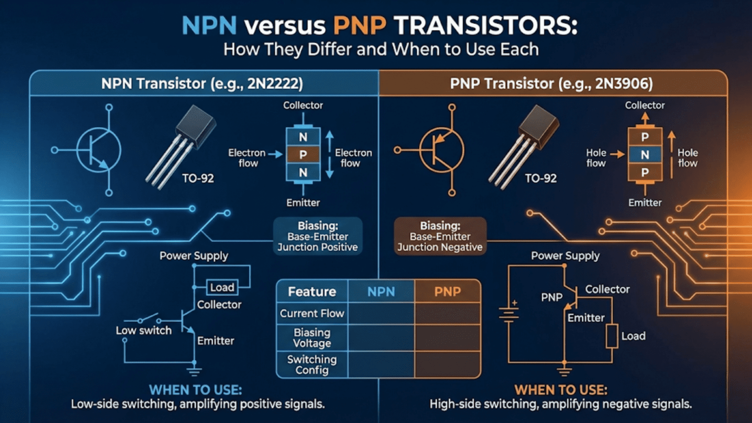
NPN and PNP transistors are complementary BJT (Bipolar Junction Transistor) types that are mirror images of each other in terms of polarity. An NPN transistor turns ON when the base is driven higher than the emitter (base current flows into the base), allowing current to flow from collector to emitter—making it ideal for low-side switching where the transistor sits between the load and ground. A PNP transistor turns ON when the base is driven lower than the emitter (base current flows out of the base), allowing current to flow from emitter to collector—making it natural for high-side switching where the transistor sits between the power supply and the load. In practice, NPN transistors are used far more commonly because they’re easier to drive from ground-referenced logic signals.
Introduction: Mirror Images in Silicon
Every BJT transistor is either NPN or PNP — two types that are complementary, meaning they perform the same function but with reversed voltage polarities and current directions. Understanding why these two types exist, exactly how they differ, and when each one is the right choice is fundamental knowledge for anyone designing or working with transistor circuits.
The distinction might seem like a minor technicality — “just use whichever one you have” — but it matters significantly in practice. Connect a PNP where an NPN is needed, apply the same base drive signal, and nothing will happen (or worse, something unexpected will). The circuit topologies, biasing arrangements, and drive signals for NPN and PNP are mirror images of each other, and mixing them up is a common source of frustration for beginners.
At the same time, both NPN and PNP transistors appear in virtually every analog circuit of any complexity, and understanding how to use them together — as complementary pairs — unlocks some of the most important circuit topologies in electronics: push-pull amplifiers, H-bridges, complementary emitter followers, and power supply circuits.
This guide develops a thorough understanding of both transistor types, systematically comparing their operation, working through practical circuits for each, explaining the memory tricks and mental models that make it easy to keep them straight, and building clear design intuition for when to reach for an NPN versus when to reach for a PNP.
The Fundamental Difference: Polarity and Carrier Type
Structure and Doping
The letters in NPN and PNP directly describe the semiconductor structure:
NPN transistor: Three semiconductor layers: N-type / P-type / N-type
- Collector: N-type (lightly doped)
- Base: P-type (very thin, lightly doped)
- Emitter: N-type (heavily doped)
PNP transistor: Three semiconductor layers: P-type / N-type / P-type
- Collector: P-type (lightly doped)
- Base: N-type (very thin, lightly doped)
- Emitter: P-type (heavily doped)
The key physical consequence: In an NPN, the majority carriers that flow through the device are electrons (negative charges), which move from emitter to collector. In a PNP, the majority carriers are holes (positive charges), which move from emitter to collector. This fundamental carrier-type difference produces the reversed polarity behavior between the two types.
Current Flow Direction
NPN transistor (conventional current):
- Collector current (I_C): Flows INTO the collector terminal
- Emitter current (I_E): Flows OUT of the emitter terminal
- Base current (I_B): Flows INTO the base terminal
- Relationship: I_E = I_C + I_B
PNP transistor (conventional current):
- Emitter current: Flows INTO the emitter terminal
- Collector current (I_C): Flows OUT of the collector terminal
- Base current (I_B): Flows OUT of the base terminal
- Relationship: I_E = I_C + I_B (magnitudes)
Memory trick — current arrows: The schematic symbols show an arrow on the emitter lead:
- NPN: Arrow points away from the base (toward the emitter terminal)
- PNP: Arrow points toward the base (away from the emitter terminal)
The arrow shows the direction of conventional current flow in the emitter. For NPN, conventional current exits the emitter (electrons enter). For PNP, conventional current enters the emitter (holes exit).
Another memory trick:
- NPN: Not Pointing iN — the emitter arrow points away from the base
- PNP: Points iN Proudly — the emitter arrow points toward the base
Voltage Polarities
NPN transistor — voltages relative to ground:
- V_E: Emitter is at the lowest potential in the transistor (usually connected to ground or near-ground)
- V_B: Base must be approximately 0.6–0.7V above the emitter (V_BE ≈ +0.6V)
- V_C: Collector must be above the emitter (V_CE > V_CE_sat ≈ 0.2V when ON)
- Summary: In NPN, collector is the most positive terminal, emitter the most negative
PNP transistor — voltages relative to supply:
- V_E: Emitter is at the highest potential in the transistor (usually connected to VCC or near-VCC)
- V_B: Base must be approximately 0.6–0.7V below the emitter (V_EB ≈ +0.6V, or V_BE ≈ -0.6V)
- V_C: Collector must be below the emitter (V_EC > V_EC_sat when ON)
- Summary: In PNP, emitter is the most positive terminal, collector the most negative
The fundamental rule:
- NPN turns ON when V_B > V_E by ~0.6V (forward bias base-emitter junction)
- PNP turns ON when V_B < V_E by ~0.6V (forward bias emitter-base junction)
NPN Transistors in Detail
The NPN as a Low-Side Switch
The most common NPN application is as a low-side switch — the transistor is placed between the load and ground:
VCC (+12V)
    │
  [Load]        ← Motor, LED, relay coil, lamp
    │
  Collector (C)
[NPN Transistor]
  Emitter (E)
    │
   GND

  Base (B)──[R_base]──Control Signal (from MCU, HIGH = ON)
How it works:
- Control signal HIGH (e.g., 5V from MCU GPIO): V_B ≈ 5V, V_E = 0V (GND), so V_BE ≈ 5V >> 0.6V threshold. Base current flows, transistor turns ON, current flows from VCC through load through transistor to GND.
- Control signal LOW (0V): V_B = 0V, V_BE = 0V, no base current, transistor OFF, no load current.
Why NPN works so naturally for low-side switching: The control signal is referenced to ground — it’s a simple HIGH/LOW logic level from a microcontroller. The emitter is at ground. Driving the base high (relative to ground) turns the transistor on. The math and the logic both work intuitively with ground-referenced control signals.
NPN Biasing for Switching
Base resistor calculation:
Given:
- VCC = 12V, load resistance R_L = 120Ω (I_C = 100mA)
- Transistor β = 100 (minimum from datasheet)
- Control signal = 5V from microcontroller GPIO
Step 1: Required base current for saturation (with overdrive) I_B_required = I_C / β = 100mA / 100 = 1mA I_B_drive = 5 × I_B_required = 5mA (5× overdrive ensures saturation)
Step 2: Base resistor R_base = (V_control – V_BE) / I_B_drive = (5V – 0.7V) / 5mA = 860Ω → Use 820Ω or 1kΩ
Step 3: Verify with chosen resistor (1kΩ) I_B = (5V – 0.7V) / 1kΩ = 4.3mA I_C_max = β × I_B = 100 × 4.3mA = 430mA >> 100mA ✓ (transistor saturates) V_CE_sat ≈ 0.2V (look up in datasheet for actual I_C)
NPN Common-Emitter Amplifier
NPN transistors in the active region (not saturated) amplify signals:
VCC (+12V)
    │
   [RC = 10kΩ]      ← Collector resistor (sets operating point)
    │
  Collector ─────── Output (AC-coupled)
[NPN Transistor]
  Emitter
    │
   [RE = 1kΩ]      ← Emitter resistor (stability/degeneration)
    │
   GND

  Base ──[R1 = 100kΩ]── VCC
  Base ──[R2 = 22kΩ]──  GND    ← Voltage divider bias
Base ──[Cin]── Input signalVoltage gain (with emitter bypass capacitor): A_v ≈ -RC / re where re = 26mV / I_C
With I_C = 1mA: re = 26Ω, A_v ≈ -10,000/26 ≈ -385 (inverting, high gain)
PNP Transistors in Detail
The PNP as a High-Side Switch
The natural PNP application is as a high-side switch — the transistor is placed between the supply and the load:
VCC (+12V)
    │
  Emitter (E)
[PNP Transistor]
  Collector (C)
    │
  [Load]             ← Motor, LED, relay coil
    │
   GND

  Base (B)──[R_base]──Control Signal
Emitter ──[R_pullup to VCC optional]How it works:
- Control signal LOW (0V): V_B = 0V, V_E = VCC = 12V, so V_BE = V_B – V_E = 0V – 12V = -12V, which means |V_BE| = 12V >> 0.6V threshold. But wait — we need V_BE = -0.6V (not +0.6V). So base being at 0V with emitter at 12V gives V_EB = 12V >> 0.6V. Transistor turns ON, current flows from VCC through emitter, through transistor, through collector, through load to GND.
- Control signal HIGH (12V, same as VCC): V_B = V_E = 12V, V_BE = 0V, no base current, transistor OFF.
The critical insight for PNP switching:
- LOW control signal = PNP ON (counter-intuitive from NPN experience)
- HIGH control signal = PNP OFF
This inversion relative to NPN is why PNP drives can seem confusing at first. A LOW signal at the base (relative to the emitter/VCC) activates the transistor.
PNP Drive Challenge: The Voltage Reference Problem
Here’s where PNP high-side switching gets tricky when driven from a microcontroller:
Scenario: MCU at 3.3V, PNP switching a 12V load.
Problem: The PNP emitter is at 12V. To turn the transistor ON, we need the base to be ~11.3V (12V – 0.7V). To turn it OFF, we need the base at 12V. But our MCU can only output 0V or 3.3V — it cannot output 11.3V or 12V!
Solutions:
Solution 1: NPN driver transistor Use a small NPN transistor to level-shift the MCU logic signal to control the PNP:
VCC (12V)
    │
[R1: 10kΩ]──────Emitter (PNP)
    │              [PNP]
  Base (PNP)      Collector ──[Load]──GND
    │
[R2: 10kΩ]
    │
  Collector (NPN)
     [NPN]
  Emitter (NPN) ── GND
    │
Base (NPN)──[R_base: 10kΩ]──MCU GPIOWhen MCU GPIO = HIGH: NPN turns ON → PNP base pulled low → PNP turns ON → Load ON When MCU GPIO = LOW: NPN turns OFF → R1 pulls PNP base to 12V → PNP turns OFF → Load OFF
Solution 2: Logic-compatible PNP with resistor network For smaller load voltages close to MCU voltage (e.g., 5V load, 3.3V MCU), a resistor network can level-shift adequately. For large voltage differences, the NPN driver approach is cleaner.
Solution 3: Use a P-channel MOSFET instead For high-side switching of moderate-voltage loads from logic, a P-channel logic-level MOSFET is often simpler than a PNP BJT. P-channel MOSFETs have similar drive challenges but gate driver ICs handle them cleanly.
PNP Biasing for High-Side Switching (Same Voltage Domain)
When MCU and load are both at 5V (common in Arduino projects):
   +5V
    │
  Emitter (E)──┐
[PNP Transistor]│
  Collector (C) │
    │           │
  [Load]       [R_pullup: 10kΩ] (keeps PNP off when MCU undriven)
    │           │
   GND          │
MCU GPIO ──[R_base: 1kΩ]──Base (B)When MCU GPIO = LOW (0V): V_E = 5V, V_B = 0V (through R_base, approximating for now) V_EB = 5V – 0V = 5V >> 0.6V → PNP turns ON Actual V_B ≈ 0V + 0.7V = 0.7V (due to V_EB drop) I_B = (5V – 0.7V) / R_base = 4.3V / 1kΩ = 4.3mA
When MCU GPIO = HIGH (5V): V_B approaches 5V through R_base, V_E = 5V V_EB ≈ 0V → PNP turns OFF ✓
Note: The 10kΩ pullup to VCC ensures the base is firmly at 5V when the MCU isn’t actively driving, preventing the transistor from floating on.
PNP Common-Emitter Amplifier
PNP amplifiers are less common than NPN but follow the same principles with inverted polarities:
   GND
    │
   [RC]           ← Collector resistor to GND (not VCC)
    │
  Collector ─── Output (AC-coupled)
[PNP Transistor]
  Emitter
    │
   [RE]
    │
   VCC             ← Emitter connects to positive supply

  Base ──[R1]── GND    ← Divider referenced to GND
  Base ──[R2]── VCC
Base ──[Cin]── Input signalThe signal inversion and gain formula are the same as NPN — only the DC biasing polarities are flipped.
Using NPN and PNP Together: Complementary Circuits
The real power of having two complementary transistor types emerges when they work together.
Push-Pull Output Stage
A push-pull output uses one NPN and one PNP to drive a load in both directions efficiently:
   VCC
    │
  Emitter
 [PNP Q1]          ← Sources current when output HIGH
  Collector
    │
    ├─────────── Output ──[Load]──GND
    │
  Collector
 [NPN Q2]          ← Sinks current when output LOW
  Emitter
    │
   GND

Input ──[to both bases]When input HIGH:
- NPN Q2 turns ON (V_BE > 0.6V), output pulled LOW
- PNP Q1 turns OFF (V_BE approaches 0)
When input LOW:
- NPN Q2 turns OFF
- PNP Q1 turns ON (V_EB > 0.6V), output pulled HIGH
Why this is better than a single transistor: A single NPN can only pull the output LOW (toward GND). A single PNP can only pull HIGH. Push-pull provides both — actively driving HIGH and actively driving LOW. This gives stronger drive capability and faster transition times because the output is never just floating.
This is the output stage of every CMOS logic gate (using MOSFETs instead of BJTs but the same topology).
Complementary Emitter Follower (Class AB Amplifier)
Similar to push-pull but with emitters at the output:
   VCC
    │
  [R_bias1]
    │
  Base/Collector of Q1
 [PNP Q1]──────────────────── Output
  Emitter                        │
    │                         [Load]
  Emitter                        │
 [NPN Q2]──────────────────── GND
  Base/Collector of Q2
    │
  [R_bias2]
    │
   GND

Input signal ──[to both bases via coupling]Properties:
- Voltage gain ≈ 1 (emitter follower configuration)
- Current gain: high (can drive low-impedance loads)
- Handles both positive and negative halves of AC signal
- Used in audio power amplifier output stages
H-Bridge for Motor Control
Four transistors (typically two NPN and two PNP, or four N-channel MOSFETs) form an H-bridge that drives a motor in both directions:
VCC
 │         │
[PNP Q1] [PNP Q2]   ← High-side drivers
 │         │
 ├───[M]───┤         ← Motor between output nodes
 │         │
[NPN Q3] [NPN Q4]   ← Low-side drivers
 │         │
GND GNDForward: Q1 + Q4 ON, Q2 + Q3 OFF → Current flows left to right through motor Reverse: Q2 + Q3 ON, Q1 + Q4 OFF → Current flows right to left through motor Brake: Q3 + Q4 ON → Both motor terminals shorted to GND (dynamic braking) Coast: All OFF → Motor freewheels
Critical rule: Never turn on both top and bottom transistors on the same side simultaneously (Q1+Q3 or Q2+Q4) — this creates a direct short from VCC to GND.
Side-by-Side: The Key Differences at a Glance
Polarity Reference
| Aspect | NPN | PNP |
|---|---|---|
| Layer structure | N-P-N | P-N-P |
| Majority carriers | Electrons | Holes |
| Emitter arrow direction | Away from base (outward) | Toward base (inward) |
| V_BE to turn on | +0.6V (base higher than emitter) | -0.6V (base lower than emitter) |
| Base current direction | Into base | Out of base |
| I_C direction | Into collector | Out of collector |
| Normal emitter connection | Near GND | Near VCC |
| Turns ON when control = | HIGH | LOW |
| Natural switching position | Low-side (between load and GND) | High-side (between VCC and load) |
Practical Usage
| Application | NPN | PNP |
|---|---|---|
| MCU-controlled switch | ✓ Directly driven (easy) | ✓ With drive circuit (harder) |
| Low-side switch | ✓ Ideal | ✗ Requires extra circuit |
| High-side switch | ✗ Requires charge pump or driver | ✓ Natural fit |
| Common-emitter amplifier | ✓ Very common | ✓ Less common |
| Emitter follower | ✓ Common | ✓ Used in push-pull |
| Push-pull output | ✓ Lower transistor | ✓ Upper transistor |
| H-bridge | ✓ Low-side pair | ✓ High-side pair |
| Frequency of use | Very common (workhorse) | Less common, specific roles |
| Complementary partners | 2N2222 + 2N2907 | BC547 + BC557 |
Practical Comparison: Same Task, Different Types
Task: Switch an LED from a 5V Microcontroller
Using NPN (low-side):
+5V ──[R_LED: 220Ω]──[LED]──Collector(C)
                              [2N2222 NPN]
                             Emitter(E)──GND
Base(B)──[R_base: 1kΩ]──MCU GPIO (HIGH = LED ON)- MCU HIGH (5V) → V_BE = 5V – 0V = 5V > 0.6V → NPN ON → LED lights ✓
- MCU LOW (0V) → V_BE = 0V → NPN OFF → LED off ✓
- Simple, direct, intuitive
Using PNP (high-side):
+5V──Emitter(E)
     [BC557 PNP]
     Collector(C)──[LED]──[R_LED: 220Ω]──GND
Base(B)──[R_base: 1kΩ]──MCU GPIO (LOW = LED ON)
(10kΩ pullup from Base to +5V to keep PNP off when MCU undriven)- MCU LOW (0V) → V_EB = 5V – 0V = 5V > 0.6V → PNP ON → LED lights ✓
- MCU HIGH (5V) → V_EB ≈ 0V → PNP OFF → LED off ✓
- Works but logic is inverted (LOW turns it on) — less intuitive
Verdict: For this task, NPN is simpler and more intuitive. PNP high-side is useful when load needs to connect to GND (e.g., negative-ground audio systems or when the LED’s cathode must be at a specific potential).
Task: Switch a 24V Relay from a 3.3V Microcontroller
Using NPN (low-side):
+24V──[Relay coil]──Collector(C)
                    [2N2222 NPN] ← handles 24V (V_CEO > 40V)
                    Emitter(E)──GND
Base(B)──[R_base: 2.2kΩ]──MCU GPIO (3.3V)
[Flyback diode across relay coil!]- MCU HIGH (3.3V) → V_BE = 3.3V – 0V = 3.3V >> 0.6V → NPN ON → Relay energizes ✓
- Simple: MCU doesn’t need to handle 24V; only the transistor does
Using PNP (high-side): Would require base voltage close to 24V to turn off, and ~23.3V to turn on. A 3.3V MCU cannot directly drive a 24V PNP — requires NPN driver stage or dedicated level-shifter circuit.
Verdict: NPN low-side switching is dramatically easier for high-voltage loads driven from low-voltage logic. This is why NPN dominates in microcontroller projects.
Selecting the Right Transistor
NPN Selection Guide
Small signal (I_C < 200mA, V_CE < 40V):
- 2N2222 / PN2222A: The most universal NPN. 600mA, 40V, β 100–300. TO-18 metal or TO-92 plastic.
- 2N3904: Very common, 200mA, 40V, β 100–300. TO-92. Slightly lower current than 2N2222.
- BC547 / BC548 / BC549: European equivalents, widely available, 100mA, 45V.
- MMBT2222 / MMBT3904: SMD SOT-23 versions of the above for PCB designs.
Medium power (200mA–2A, V_CE up to 80V):
- BD139: 1.5A, 80V, TO-126. Good for moderate power.
- BC337: 800mA, 45V, TO-92. Step up from BC547.
- TIP31C: 3A, 100V, TO-220. Larger switch applications.
High power (>2A):
- 2N3055: Classic, 15A, 60V, TO-3 metal case. Used since the 1960s.
- TIP35C: 25A, 100V, TO-247.
PNP Selection Guide
Small signal (complementary pairs):
- 2N2907 / PN2907A: PNP complement to 2N2222. 600mA, 40V.
- 2N3906: PNP complement to 2N3904. 200mA, 40V.
- BC557 / BC558 / BC559: PNP equivalents to BC547 series.
- MMBT2907 / MMBT3906: SOT-23 SMD versions.
Medium power:
- BD140: PNP complement to BD139. 1.5A, 80V.
- TIP32C: PNP complement to TIP31C. 3A, 100V.
High power:
- MJ2955: PNP complement to 2N3055. 15A, 60V.
- TIP36C: PNP complement to TIP35C. 25A, 100V.
Reading Transistor Datasheets
Key parameters to check:
- β (hFE): Current gain, often specified at a specific I_C. Varies with operating conditions.
- V_CEO: Maximum collector-emitter voltage (base open). Must exceed your supply voltage.
- I_C max: Maximum continuous collector current.
- P_total: Maximum power dissipation (with/without heatsink).
- V_BE_sat: Base-emitter saturation voltage (affects base resistor calculation).
- V_CE_sat: Collector-emitter saturation voltage (determines on-state losses).
- f_T: Unity gain bandwidth — important for RF and high-speed applications.
Common Mistakes When Using NPN and PNP
Mistake 1: Connecting PNP Like an NPN
Symptom: Circuit doesn’t work; transistor may get hot.
What happened: Applied a HIGH signal to control a PNP the same way as an NPN. PNP needs LOW to turn on; a HIGH signal either turns it off or applies the wrong polarity of V_BE.
Fix: Invert the control logic, or redesign with NPN.
Mistake 2: Forgetting That PNP Turns ON with LOW
Symptom: LED or load works backwards — on when expected off, off when expected on.
What happened: PNP’s inverted logic not accounted for in firmware or hardware.
Fix: In firmware, invert the output logic for PNP-switched loads. Or redesign the control circuit with an NPN driver stage that re-inverts.
Mistake 3: Insufficient Base Overdrive
Symptom: Transistor gets very warm; V_CE much higher than expected (> 1V instead of 0.2V); load doesn’t receive full voltage.
What happened: Transistor not fully in saturation — operating in active region instead. V_CE in active region = V_CE_sat would be very low; higher V_CE means it’s not fully on.
Fix: Increase base current. Use at least 5–10× more base current than I_C/β minimum. Check β at actual operating current (β drops at high I_C).
Mistake 4: No Flyback Diode on Inductive Load
Symptom: Transistor fails immediately or after brief operation when switching motors, relays, or solenoids.
What happened: Inductive kickback voltage spike destroyed the transistor.
Fix: Always add a flyback diode across any inductive load. For NPN low-side: diode cathode to VCC, anode to collector. For PNP high-side: diode anode to GND, cathode to collector.
Mistake 5: Using Standard Transistor with 3.3V MCU
Symptom: Transistor barely turns on with 3.3V logic; V_CE_sat too high; doesn’t switch cleanly.
What happened: Some transistors need V_BE of 0.7–0.8V to fully saturate. With 3.3V logic and base resistor, actual V_BE may be only 0.6–0.65V — insufficient for clean saturation.
Fix: Check datasheet’s V_BE_sat specification. Reduce base resistor slightly to increase base current. Or choose transistors specifically characterized for 3.3V logic drive (some datasheets specify hFE at low V_BE).
Comparison Table: NPN vs. PNP Complete Reference
| Property | NPN | PNP |
|---|---|---|
| Semiconductor layers | N-P-N | P-N-P |
| Primary charge carrier | Electrons | Holes |
| Emitter arrow | Points away from base | Points toward base |
| ON condition | V_B > V_E + 0.6V | V_B < V_E – 0.6V |
| Base current direction | Into base terminal | Out of base terminal |
| Collector current direction | Into collector | Out of collector |
| Emitter reference | Connected near GND | Connected near VCC |
| Control polarity | HIGH = ON | LOW = ON |
| Natural switch position | Low-side | High-side |
| Direct MCU drive (3.3/5V) | Easy (emitter to GND) | Requires drive circuit (unless same voltage) |
| Common amplifier config | Common-emitter (very common) | Common-emitter (less common) |
| Push-pull role | Lower transistor (sinks current) | Upper transistor (sources current) |
| H-bridge role | Low-side pair | High-side pair |
| Availability | Very common, wide selection | Common, complementary pairs |
| General frequency of use | Dominant (majority of designs) | Supporting role, specific applications |
| Complementary pair examples | 2N2222, 2N3904, BC547 | 2N2907, 2N3906, BC557 |
Conclusion: Two Types, One Complementary System
NPN and PNP transistors are not competitors — they are complementary tools designed to work together. NPN is the workhorse of digital switching, low-side control, and most amplifier designs, and its behavior aligns naturally with ground-referenced logic signals. PNP fills the complementary role: high-side switching, push-pull outputs, and as the upper transistor in bridge circuits.
Practical Decision Framework
When deciding between NPN and PNP, ask three questions:
1. Where should the transistor sit in the circuit?
- Between load and GND (low-side switch) → NPN
- Between supply and load (high-side switch) → PNP (or P-channel MOSFET)
2. What drives the control signal?
- Ground-referenced logic (MCU GPIO, 0V/3.3V or 0V/5V) → NPN (straightforward)
- Supply-referenced signal or need HIGH to turn on → PNP with drive circuit, or reconsider topology
3. Is this part of a complementary circuit?
- Push-pull output, H-bridge, Class AB amplifier → Both NPN and PNP, each in appropriate role
The 80/20 Rule
For approximately 80% of hobbyist and light professional applications, NPN transistors are the right choice. The BCxx7, 2N2222, or 2N3904 family will cover most switching and amplification needs. PNP transistors appear in specific situations — high-side switching, push-pull outputs, and complementary amplifier stages — where their characteristics are genuinely needed rather than merely convenient.
Master the NPN first: understand its biasing, its saturation requirements, its low-side switching topology. Then layer in PNP for the complementary applications where it shines. Together, they provide the building blocks for nearly every BJT circuit you’ll encounter.
The letters spell out the layers — NPN and PNP. But what they represent is simpler than the jargon: one type for pulling signals toward ground, the other for pulling them toward the supply. Both serving the same fundamental purpose — using a small signal to control a large one — just from opposite ends of the circuit.