The most common soldering mistakes are cold (dry) joints caused by insufficient heat or movement during cooling, solder bridges that short adjacent pads, insufficient or excessive solder volume, overheated components from too much heat or prolonged iron contact, and lifted PCB pads from mechanical stress while hot. Most of these mistakes stem from three root causes: incorrect temperature, incorrect technique (heating the iron rather than the joint), or using too little flux—meaning the majority of soldering problems can be prevented by mastering basic technique before attempting complex work.
Introduction: Why Mistakes Happen and Why They Matter
Learning to solder means learning to make mistakes. Even experienced solderers occasionally produce cold joints, create unwanted bridges, or lift a pad. The difference between a beginner and an expert isn’t the absence of mistakes—it’s recognizing them immediately, understanding why they happened, and knowing exactly how to fix them.
Soldering mistakes matter far more than they might appear to. A joint that looks slightly rough might seem like a minor cosmetic issue, but a cold solder joint can have resistance hundreds of times higher than a good joint, causing voltage drops, heat generation, and intermittent failures that are notoriously difficult to debug. A solder bridge might be nearly invisible to the naked eye but creates a dead short that destroys components the moment power is applied. A lifted pad that seems like a minor inconvenience requires time-consuming PCB repair or, in severe cases, scraps an entire board.
Understanding common soldering mistakes deeply—not just what they look like but why they happen physically—is the fastest route to eliminating them from your work. Many beginners treat soldering problems as random and unpredictable. In reality, each defect has specific root causes that, once understood, become easy to avoid consistently.
This comprehensive guide examines every major category of soldering mistake in detail. For each, we explain what it looks like, what physical process caused it, why it matters electrically and mechanically, how to fix existing instances, and most importantly, how to prevent it from occurring in the first place. We also address mistakes beyond the joint itself—component placement errors, tool misuse, workspace hazards, and workflow problems that create compounding difficulties.
Whether you’re troubleshooting a circuit that mysteriously doesn’t work, trying to improve the consistency of your finished boards, or preparing to attempt more demanding soldering work, understanding these mistakes and their remedies will substantially accelerate your development as a solderer.
Category 1: Solder Joint Quality Mistakes
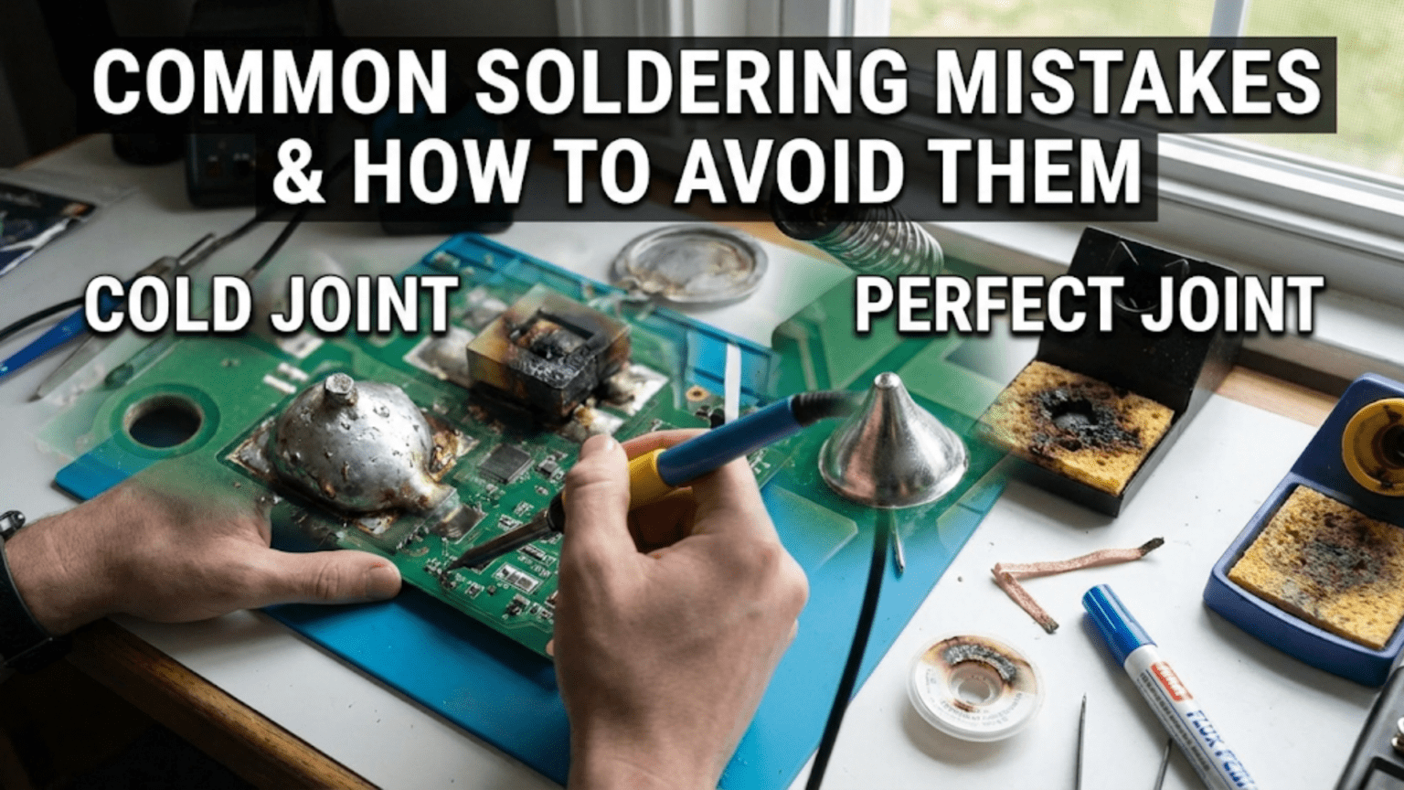
Mistake 1: Cold (Dry) Joints
What it looks like: A cold joint appears dull, grainy, or frosted rather than smooth and shiny (for leaded solder). The solder surface looks rough and matte, often with a granular crystalline texture. The solder may appear to be sitting on the surface rather than flowing around the lead and pad.
What caused it: Cold joints result from the solder solidifying before it properly wet the surfaces. The most common causes are:
- Insufficient heat: The joint—either the pad, the component lead, or both—wasn’t hot enough when solder was applied
- Heating the iron, not the joint: Solder applied to the iron tip instead of the joint melts but doesn’t flow properly into the connection
- Movement during cooling: The joint was disturbed while the solder was in its pasty semi-solid state between molten and fully solid, disrupting the crystal formation
- Contaminated surfaces: Oxidation or contamination prevented proper wetting even with adequate heat
- Expired or degraded flux: Old solder wire or flux-depleted solder doesn’t provide adequate chemical cleaning during the process
Why it matters: Cold joints are the most dangerous soldering defect because they often appear to work initially. The solder makes physical contact, so a resistance test might show continuity. But cold joints have much higher resistance than good joints (sometimes 10–1000× higher), generate heat in operation, and degrade over time. In vibrating environments or through thermal cycling, cold joints fail entirely—often intermittently, making them among the hardest defects to locate when debugging.
How to fix it:
- Apply fresh flux directly to the joint (flux pen or liquid flux)
- Place the iron tip on the joint, contacting both pad and lead
- Allow 1–3 seconds for the joint to reheat fully
- Watch for the solder to flow and reflow into a shiny, smooth surface
- Remove the iron and allow to cool completely without movement
How to prevent it:
- Always heat both the pad and the component lead simultaneously with the iron
- Apply solder to the joint, not to the iron tip
- Use adequate iron temperature (not too low)
- Hold the joint completely still until it has fully solidified (3–5 seconds)
- Use fresh solder with active flux core
- Add external flux for difficult joints or older components
Mistake 2: Disturbed Joints
What it looks like: Similar to a cold joint—dull, rough, possibly cracked surface—but the cause is different. A disturbed joint often has an uneven or wrinkled surface, sometimes with visible crystalline texture or radial cracks from the lead outward.
What caused it: Disturbed joints happen when the joint is moved or vibrated while the solder is in the pasty transition state between fully liquid and fully solid. At this stage, the solder’s grain structure is forming, and any disruption to that structure creates a permanently deformed microstructure.
Common causes include:
- PCB moved or bumped while joints are cooling
- Component lead touched or moved immediately after iron removal
- Hand tremor while removing the iron
- Vibration from nearby equipment during cooling
- Attempting to test the joint (pressing on it) before it’s fully solid
Why it matters: Disturbed joints share the same reliability concerns as cold joints—high resistance, poor mechanical strength, and susceptibility to failure under stress. They can be harder to identify visually because they may have some shininess if the metal surface was previously clean.
How to fix it: Same as cold joint repair: add flux, reheat fully, allow to solidify without movement.
How to prevent it:
- Don’t touch the PCB or component leads for at least 5 seconds after removing the iron
- Work on a stable, vibration-free surface
- Remove the iron with a smooth, steady motion—no twisting or dragging
- Don’t blow on joints to cool them faster
Mistake 3: Solder Bridges
What it looks like: A tiny blob, strand, or filament of solder connecting two pads, traces, or component leads that should be electrically isolated from each other. On fine-pitch ICs or connectors, bridges can be nearly invisible without magnification.
What caused it: Solder bridges typically form when:
- Too much solder was applied: Excess solder flows toward adjacent pads during application or cooling
- Iron dragged across pads: Moving the iron tip across several pads while still laden with solder deposits a trail of metal
- Solder wicked between pads: Surface tension pulls molten solder toward adjacent surfaces, especially on fine-pitch work
- Contaminated tip: A tip carrying a large ball of solder can deposit bridges when touched to a pad
Why it matters: Solder bridges are short circuits. In the best case, they prevent the circuit from functioning. In the worst case, they destroy components or cause fires when power is applied. A bridge between VCC and GND is the most dangerous scenario, potentially exploding capacitors or burning out regulators. Even bridges between signal lines create incorrect behavior that may be difficult to trace.
How to fix it: Method 1: Reflow with flux (often sufficient for small bridges)
- Apply additional flux to the bridge
- Touch the iron briefly to the bridge—the liquid solder often retracts onto the pads
- Inspect under magnification
Method 2: Desoldering wick
- Apply fresh flux to the bridge
- Place desoldering wick directly over the bridge
- Press the iron on top of the wick with moderate pressure
- Allow 2–3 seconds for the wick to absorb the solder
- Lift the wick and iron together (don’t drag—it may lift the pad)
- Inspect; repeat if necessary
Method 3: Desoldering pump Best for larger bridges; less precise than wick on fine-pitch work.
How to prevent it:
- Use an appropriate amount of solder—err on the side of less
- For fine-pitch work, use a smaller diameter solder wire (0.5–0.6mm)
- Keep the iron tip clean and properly tinned
- For ICs with many fine-pitch pins, consider using flux-and-drag technique
- Inspect every joint with magnification, especially on fine-pitch components
Mistake 4: Insufficient Solder (Starved Joint)
What it looks like: The solder fillet is thin, incomplete, or barely covers the pad. In through-hole work, the hole may not be completely filled. The concave fillet shape that a good joint forms is absent—instead, just a thin coating or partial connection appears. The component lead may be visible through gaps in the solder.
What caused it:
- Not enough solder wire fed to the joint
- Iron removed before solder fully filled the joint
- Solder did not flow into the through-hole (pad not hot enough)
- Solder wicked away along a long component lead
Why it matters: Insufficient solder reduces both the mechanical strength and the cross-sectional area of the electrical connection. A starved joint is more likely to fracture under vibration or thermal stress. On through-hole joints, the solder is meant to fill the plated through-hole barrel, creating a connection on both board sides—insufficient solder may fail to achieve this.
How to fix it:
- Apply flux to the existing joint
- Reheat fully
- Feed additional solder while the joint is hot
- Remove iron, allow to cool
How to prevent it:
- Watch the solder flow as you apply it and continue until a complete fillet forms
- For through-hole work, verify solder appears on the component side (top) of the board, indicating the hole is filled
- Use solder wire of appropriate diameter—very fine wire (0.3mm) requires more feeding per joint
Mistake 5: Excessive Solder (Oversoldered Joint)
What it looks like: A large, rounded blob of solder sitting on the pad, often obscuring the component lead entirely. The joint looks like a ball rather than a smooth fillet. May touch adjacent pads or components.
What caused it:
- Too much solder wire fed to the joint
- Slow or hesitant feeding without watching the joint’s state
- Difficulty controlling thin solder wire that feeds quickly
Why it matters: Beyond creating bridges to adjacent pads, excessive solder hides the joint’s actual condition—you can’t see whether the solder properly wet the pad and lead under the blob. It wastes material and looks unprofessional. Excessively large joints also have more thermal mass, making them harder to rework later.
How to fix it:
- Apply flux to the excess
- Use desoldering wick to remove the excess
- Alternatively, heat the joint and use a solder sucker to remove the excess
How to prevent it:
- Feed solder slowly and deliberately
- Watch the joint develop—stop adding solder when the fillet looks complete
- Practice portion control on scrap boards to develop feel for the right amount
- Use appropriate wire diameter for the work
Mistake 6: Solder Balls and Solder Splatter
What it looks like: Small spheres or droplets of solder deposited randomly on the PCB surface, away from intended joints. They may be on silkscreen areas, between pads, or on nearby components.
What caused it:
- Temperature too high causing solder to spit or spatter
- Moisture in solder wire or flux (boils explosively when heated)
- Iron tip slipping and flicking solder
- Solder wire fed too quickly to a very hot iron tip
Why it matters: Solder balls can create bridges if they land between pads. Even if they don’t create immediate shorts, they can shift under vibration and cause intermittent connections. They’re a sign that soldering conditions weren’t optimal.
How to fix it: Solder balls not touching any pads can be removed with a brush or tape (low-tack). Those near pads need careful removal with a soldering iron or desoldering wick.
How to prevent it:
- Reduce iron temperature slightly if spattering occurs
- Use fresh, dry solder (store in a cool, dry environment)
- Add solder more slowly to a hot iron
- Keep tip at appropriate temperature—not excessively high
Mistake 7: Icicles and Spikes
What it looks like: Sharp points or spikes of solder protruding from the joint, rather than smooth rounded fillets. The solder appears to have been pulled into a point as the iron was removed.
What caused it:
- Iron removed too quickly while solder was still sticky/semi-solid
- Iron dragged along the joint rather than lifted cleanly
- Insufficient flux, causing poor flow characteristics
- Temperature too low, so solder was viscous when iron departed
Why it matters: Icicles can create bridges to adjacent features. They also indicate poor technique or flux condition that likely means the joint itself is also defective underneath.
How to fix it: Add flux and reflow the joint. The icicle should retract and smooth out when solder fully liquefies again.
How to prevent it:
- Remove the iron with a smooth, clean lifting motion—not dragging
- Ensure adequate flux is present
- Work at appropriate temperature
- Allow full dwell time for solder to become fully liquid before removing iron
Category 2: Component and Placement Mistakes
Mistake 8: Wrong Component Polarity
What it looks like: Component installed backward—stripe on diode facing wrong direction, longer LED lead in wrong hole, electrolytic capacitor with positive lead in negative hole, IC installed 180° rotated.
What caused it:
- Not checking orientation markings before soldering
- Misreading schematic or PCB silkscreen
- Rushing through assembly
- Assuming polarity based on position rather than marking
Why it matters: This is potentially the most damaging mistake in this list:
- Diodes/rectifiers: Circuit simply won’t work (blocks current in intended direction)
- LEDs: Won’t light up; may be damaged under reverse voltage
- Electrolytic capacitors: Can explode violently under reverse polarity—a dangerous failure mode
- ICs: Instant destruction when power is applied—most ICs don’t survive reverse supply polarity
- Transistors: Circuit malfunction or device damage depending on type
How to fix it: Desolder the component and reinstall correctly. This is far preferable to the consequence of powering the circuit with reversed components.
How to prevent it:
- Before placing any polarized component, identify its positive and negative terminals physically
- Match those terminals to the PCB markings (look for + symbols, stripes, pin 1 indicators)
- Establish a personal checkpoint: before every polarized component, pause and verify
- Consider using component color coding or marking during assembly
- Do a final visual inspection of all polarized components before applying power for the first time
Mistake 9: Wrong Component Value
What it looks like: Correct component type in the correct location but with wrong specifications—wrong resistance, wrong capacitance, wrong voltage rating, wrong current rating.
What caused it:
- Resistor color bands misread
- Components from different reels/bags mixed up
- Reading schematic incorrectly
- Using similar-looking components interchangeably without checking
Why it matters: Wrong values cause incorrect circuit behavior ranging from subtle performance degradation to catastrophic failure. A 10Ω resistor where 10kΩ belongs will pass 1000× more current, likely burning out components. A capacitor with insufficient voltage rating may fail catastrophically.
How to prevent it:
- Measure resistors with a multimeter before installing
- Keep components clearly organized, never mixed
- Double-check value against BOM (Bill of Materials) or schematic for each component before placement
- Particularly verify any resistors by measurement—color codes are easy to misread
Mistake 10: Component Not Seated Properly
What it looks like: Component body sitting away from the PCB surface, leads not fully inserted through holes, component tilted or leaning.
What caused it:
- Leads not pushed fully through holes before soldering
- Lead bent under the board preventing full insertion
- Not checking seating before soldering
Why it matters: Improperly seated components may fail mechanically (joint stressed at unusual angle), create clearance issues with enclosures or other components, or in the case of heat-generating components, prevent proper thermal conduction.
How to fix it: Desolder, correct seating, resolder. Attempting to push a component flat after soldering risks lifting pads.
How to prevent it:
- Check that all leads are fully inserted before soldering
- Verify the component body is flush with the board (or at intended standoff height)
- Use a component holder or tape to maintain position while soldering
Category 3: Pad and PCB Damage Mistakes
Mistake 11: Lifted Pads
What it looks like: The copper pad peels away from the PCB substrate, sometimes entirely detaching and sticking to the component lead. The board surface shows a bare, pale area where the pad used to be, often with an exposed trace leading to it.
What caused it:
- Excessive heat: Prolonged heat weakens the adhesive bond between copper and substrate
- Mechanical force while hot: Pushing, pulling, or twisting leads while the joint is hot
- Repeated rework: Each rework cycle weakens the pad bonding
- Aggressive desoldering: Solder wick or pump creating strong mechanical pull on a hot pad
- Poor PCB quality: Thin copper or weak adhesion in budget boards
Why it matters: A lifted pad breaks the circuit trace. Fixing it requires PCB repair (soldering a jumper wire to the nearest accessible trace point), which is time-consuming and weakens the board. In fine-pitch or high-density boards, repair may be impossible.
How to fix it:
- Don’t panic—most lifted pads are repairable
- Identify where the trace runs that connected to the lifted pad
- Scrape or clean a small section of the trace nearby
- Solder a fine wire from the component lead to the exposed trace
- Or use conductive epoxy to re-adhere the pad, then solder carefully
How to prevent it:
- Keep iron dwell time short—5 seconds maximum for most joints
- Never apply force to a joint while it’s hot
- Keep iron temperature appropriate—too hot accelerates pad delamination
- Limit rework attempts on the same pad (maximum 2–3 times)
- Use quality PCBs with proper copper weight and substrate adhesion
Mistake 12: Burned or Delaminated PCB
What it looks like: The PCB substrate material appears discolored (brown, dark, or charred) around a joint. In severe cases, the substrate may crack, warp, or separate into layers (delamination).
What caused it:
- Iron temperature far too high
- Extremely prolonged iron contact
- Touching the iron to the bare substrate (not the pad)
Why it matters: PCB substrate damage is usually irreversible. Burned substrate may also absorb moisture more readily, degrading electrical insulation. Delaminated boards have compromised structural integrity and may develop opens in internal layers.
How to prevent it:
- Use appropriate iron temperature
- Never exceed 5 seconds of iron contact in a single attempt
- If a joint isn’t flowing, remove, allow to cool, add flux, and retry
- Never apply the iron directly to the PCB substrate—only to pads and leads
Mistake 13: Damaged Traces
What it looks like: PCB copper trace scraped, cut, or lifted along its length—distinct from a lifted pad, which is at the component connection point. Trace damage appears as a gap or scratch in the copper path.
What caused it:
- Slipping iron tip scratching across traces
- Mechanical abrasion during handling or lead trimming
- Overzealous cleaning with abrasive materials
Why it matters: Trace damage creates open circuits exactly as a lifted pad does. Depending on the trace’s current-carrying role, the damage may go unnoticed until a critical moment or may cause immediate circuit failure.
How to fix it: Bridge small trace cuts with a thin wire soldered across the gap, or use specialized PCB trace repair products (conductive paint).
How to prevent it:
- Work carefully with the iron, especially near fine traces
- Use gentleness when handling completed boards
- Flush-cut leads carefully with properly positioned cutters
Category 4: Tool and Setup Mistakes
Mistake 14: Wrong Iron Temperature
What it looks like: Too cold: solder doesn’t flow, joints look grainy, requires long contact time. Too hot: flux burns immediately, PCB discolors, components may be damaged, solder spatters.
Correct ranges:
- Leaded solder: 315–360°C
- Lead-free solder: 350–400°C
- Fine/delicate work: Lower end
- Large pads / ground planes: Upper end
What caused it:
- Cheap iron with no temperature control
- Incorrect temperature setting
- Tip degradation causing poor heat transfer (feels cold, needs higher setting)
- Heavy tip or large thermal mass work requiring higher temperature
Why it matters: Temperature is one of the most fundamental variables in soldering. Too cold → cold joints and PCB damage from prolonged contact. Too hot → component damage, PCB damage, flux burnoff before wetting occurs, and tip oxidation.
How to prevent it:
- Use a temperature-controlled station—the single most important equipment investment
- Calibrate periodically using a tip thermometer
- Replace tips that require increasingly high temperatures to function
- Know your solder’s melting point and work 150–200°C above it
Mistake 15: Dirty or Unloaded Tip
What it looks like: Tip appears dark brown or black, possibly pitted. Solder balls up on the tip instead of flowing smoothly. Heat transfer to joints seems poor. Solder doesn’t wet the tip properly.
What caused it:
- Not cleaning the tip during use
- Leaving the iron on without work for extended periods (tip oxidizes)
- Using wrong cleaning method (abrasive files that damage the plating)
- Not tinning the tip before storing or shutting off
Why it matters: An oxidized or contaminated tip transfers heat poorly and inconsistently. A tip that solder won’t wet will deposit solder poorly onto joints. Poor heat transfer forces longer contact times, increasing risk of PCB and component damage.
How to fix it:
- Attempt cleaning with brass wool tip cleaner
- Apply fresh solder and clean again
- Use tip tinner/activator compound for severely oxidized tips
- Replace tip if it won’t accept tin even after treatment
How to prevent it:
- Clean the tip every few joints during use
- Tin the tip whenever you set the iron down
- Always tin the tip before switching the iron off
- Use brass wool rather than wet sponges (less thermal shock to tip)
- Store irons with a tinned tip
Mistake 16: Incorrect Solder Wire Diameter
What it looks like: Using wire that’s too thick makes it difficult to control the amount deposited, especially on fine-pitch work. Using wire that’s too thin makes it tedious and slow for large joints or connectors.
Optimal diameters:
- SMD fine-pitch work: 0.5mm
- General through-hole: 0.6–0.8mm
- Large connectors and wires: 1.0–1.5mm
How to prevent it: Keep a few diameters on hand and choose the one appropriate for the current work.
Mistake 17: Inadequate Flux
What it looks like: Joints that won’t wet, that look dull even after good technique, or that require excessively long iron contact to achieve flow. Cold joints despite correct technique.
What caused it:
- Old solder wire with degraded flux core
- Not adding external flux when attempting rework
- Working with oxidized or contaminated surfaces without extra flux
Why it matters: Flux is not optional—it’s chemically essential for solder to wet surfaces. Without adequate flux, even perfect technique produces poor joints.
How to prevent it:
- Use fresh solder with active flux core
- Add flux pen or liquid flux for any rework operation
- Add flux when working on old, oxidized components or boards
- Apply flux whenever a joint isn’t flowing properly—before retrying
Category 5: Workflow and Process Mistakes
Mistake 18: Soldering Without a PCB Holder
What it looks like (the consequence): Hands trembling or awkward because one hand holds the PCB, one holds the iron, and there’s no way to hold the solder wire. Components fall out of holes. Joints disturbed during cooling when PCB is set down.
What caused it: Attempting to solder without a proper third-hand tool, PCB vise, or holder.
Why it matters: Stable work is the foundation of consistent soldering. Unstable boards lead to disturbed joints, dropped components, poor iron contact angles, and physically uncomfortable positions that impair fine motor control.
How to prevent it: Invest in a PCB holder or helping-hands device. This is inexpensive and immediately improves results. For larger boards, a dedicated PCB bench vise is ideal.
Mistake 19: Poor Lighting and Magnification
What it looks like: Missing solder bridges on fine-pitch ICs, not noticing cold joints, mistaking acceptable lead-free dullness for a problem and overheating joints trying to make them shiny.
What caused it: Working under inadequate lighting or without magnification, especially for fine work.
How to prevent it: Bright, adjustable task lighting and at least a simple 3–5× magnifier (loupe or stand magnifier) catches most visual defects. Invest in good lighting—it costs little and helps enormously.
Mistake 20: Applying Power Before Visual Inspection
What it looks like: The consequences: burned components, exploding capacitors (from reverse polarity), blown fuses, damaged power supplies, or simply a circuit that doesn’t work and now has additional damage making troubleshooting harder.
What caused it: Eagerness to see the circuit work, skipping systematic inspection.
Why it matters: This is the mistake that turns fixable assembly errors into component replacement projects. A reversed electrolytic capacitor that’s visually obvious takes 5 minutes to fix before power-up. After power-up, it may have vented electrolyte onto the board, destroying other components, and requiring extensive cleaning in addition to replacement.
How to prevent it: Before any first power application:
- Inspect all polarized components for correct orientation
- Check for obvious solder bridges (especially around ICs and connectors)
- Verify supply connections (correct polarity)
- Measure resistance between supply rails with a multimeter—very low resistance (near zero) indicates a short
- If possible, use a current-limited bench power supply for first power-up
Mistake 21: Not Cleaning Flux Residue
What it looks like: Brown or yellowish residue around solder joints, which may be sticky, and in humid environments may support electrical leakage between closely spaced conductors.
What caused it: Skipping post-soldering cleaning.
Why it matters: For most “no-clean” flux formulations used in hobby soldering, residue is not electrically harmful and doesn’t need removal. However, in high-humidity environments, near high-voltage traces, on precision sensor circuits, or when conformal coating is to be applied, flux residue must be removed.
How to fix it: Clean with 91% or higher isopropyl alcohol (IPA) and a stiff brush (toothbrush works well). For stubborn residue, flux remover solvents are available. Rinse with fresh IPA and allow to dry completely.
How to prevent it: Establish a cleaning step as part of your assembly workflow, especially for sensitive circuits.
Comparison Table: Soldering Defects at a Glance
| Defect | Visual Appearance | Root Cause | Electrical Effect | Difficulty to Fix | Prevention Priority |
|---|---|---|---|---|---|
| Cold joint | Dull, grainy, rough surface | Insufficient heat / movement during cooling | High resistance, intermittent failure | Easy (reflowing) | High |
| Solder bridge | Solder connecting adjacent pads | Too much solder, poor technique | Short circuit | Easy to moderate | Critical |
| Insufficient solder | Thin, incomplete fillet | Too little solder applied | Weak joint, potential open | Easy (add solder) | Medium |
| Excessive solder | Large blob, rounded mass | Too much solder applied | Bridges possible, hides defects | Moderate (remove excess) | Medium |
| Lifted pad | Missing copper pad, exposed substrate | Excessive heat or mechanical force | Open circuit | Difficult (jumper wire repair) | High |
| Disturbed joint | Rough, cracked, wrinkled surface | Movement during cooling | High resistance, intermittent | Easy (reflow) | High |
| Wrong polarity | Component backwards | Not checking orientation | Circuit failure, component damage | Easy if caught early | Critical |
| Oxidized tip | Dark, solder won’t wet tip | Lack of tip maintenance | Inconsistent heat transfer | Easy (tip cleaning) | High |
| Solder balls | Random solder spheres on board | Temperature too high, moisture | Potential bridges | Moderate (removal) | Medium |
| Icicles / spikes | Sharp solder points | Poor iron departure, low flux | Potential bridges | Easy (reflow with flux) | Medium |
| Burned PCB | Dark, discolored substrate | Excessive temperature / time | Substrate degradation | Irreversible | Critical |
| Trace damage | Scratch or gap in copper trace | Mechanical or iron slip | Open circuit | Moderate (jumper repair) | Medium |
Systematic Approach to Troubleshooting Solder Problems
When Your Circuit Doesn’t Work
Many electronics troubleshooting sessions trace back to soldering defects rather than design errors. A systematic approach to ruling out soldering problems saves significant time.
Step 1: Visual inspection before power With good lighting and magnification, examine every joint on the board. Look for:
- Dull, grainy joints (cold)
- Bridges between pads
- Missing joints (component lead not in hole, or not soldered)
- Reversed components (polarity markers)
Step 2: Resistance check before power Measure resistance between supply rails (VCC and GND). Near-zero resistance indicates a short circuit—find it before applying power.
Step 3: Probe the circuit with power If visual inspection finds nothing and resistance check passes, apply power carefully. Use a current-limited supply if available. Measure voltages at key nodes—unexpected zeros or incorrect voltages point to open circuits (cold joints) or shorts (bridges).
Step 4: Target suspected areas If a specific function doesn’t work, focus inspection on components relevant to that function. Cold joints are often localized around specific components that were difficult to solder (large pins, ground planes, connectors).
Step 5: Reflow-and-test cycle If a cold joint is suspected but not visible, applying fresh flux and reflowing all joints in the suspected area often resolves intermittent issues without requiring precise identification of the specific bad joint.
Building a Quality Mindset
The best approach to soldering mistakes is developing a mindset that prevents them rather than fixing them:
Inspect before proceeding: Check each joint before moving to the next. Catching a cold joint immediately is much easier than hunting for it later.
Understand the why: Every technique in soldering has a physical reason. Understanding why you heat both surfaces, why you remove the iron before solder, and why you wait for cooling makes you adaptive to new situations rather than dependent on memorized rules.
High standards from the start: It’s tempting to accept “good enough” joints when learning. But developing high standards early establishes habits that produce consistently good work without extra effort.
Embrace rework: Reflowing or redoing a bad joint isn’t failure—it’s quality control. Professional assembly has inspection and rework as standard steps. Don’t let perfectionism prevent you from fixing identifiable defects.
Conclusion: From Mistakes to Mastery
Every mistake in this guide is correctable, and with proper technique, most are entirely preventable. The most important insight is that soldering mistakes are not random—they have specific physical causes that, once understood, can be systematically eliminated.
The Three Root Causes Behind Almost All Defects
If you internalize nothing else from this article, remember:
1. Insufficient heat / incorrect heating technique Accounts for cold joints, disturbed joints, icicles, and poor wetting. Fix: heat both surfaces, not the iron alone.
2. Incorrect solder quantity Accounts for bridges, starved joints, solder balls, and oversolder. Fix: watch the joint as solder flows, stop at the right amount.
3. Inadequate flux Amplifies nearly every other problem. Fix: use fresh solder and add extra flux for any challenging work.
The Development Path
Early learning (first weeks): Focus on avoiding cold joints and bridges. These are the most common and most consequential beginner errors. Master the fundamental technique of heating the joint—not the iron—and watch joints for proper wetting.
Intermediate (months 2–4): Develop consistent solder quantity control, add magnification inspection to your workflow, and begin working on finer-pitch components.
Advanced (month 6+): Troubleshoot circuits using soldering knowledge, tackle SMD work, develop rework skills, and build a systematic pre-power-up checklist.
Final Thought
Soldering mistakes are part of learning. Every experienced solderer has stories of lifted pads, reversed ICs, and mysterious bridges. What separates experienced from inexperienced solderers isn’t the absence of mistakes—it’s catching them early, understanding why they happened, fixing them correctly, and adjusting technique to prevent recurrence.
Build that feedback loop—observe, understand, adjust—and your mistake rate will drop rapidly. The joints that once required two or three attempts begin forming perfectly on the first try. The troubleshooting that once consumed hours becomes a quick inspection. The craft that once felt mysterious becomes second nature.
Good soldering takes minutes to learn, a lifetime to master, and produces connections that last for decades. Avoid these mistakes, embrace the craft, and build circuits that work.