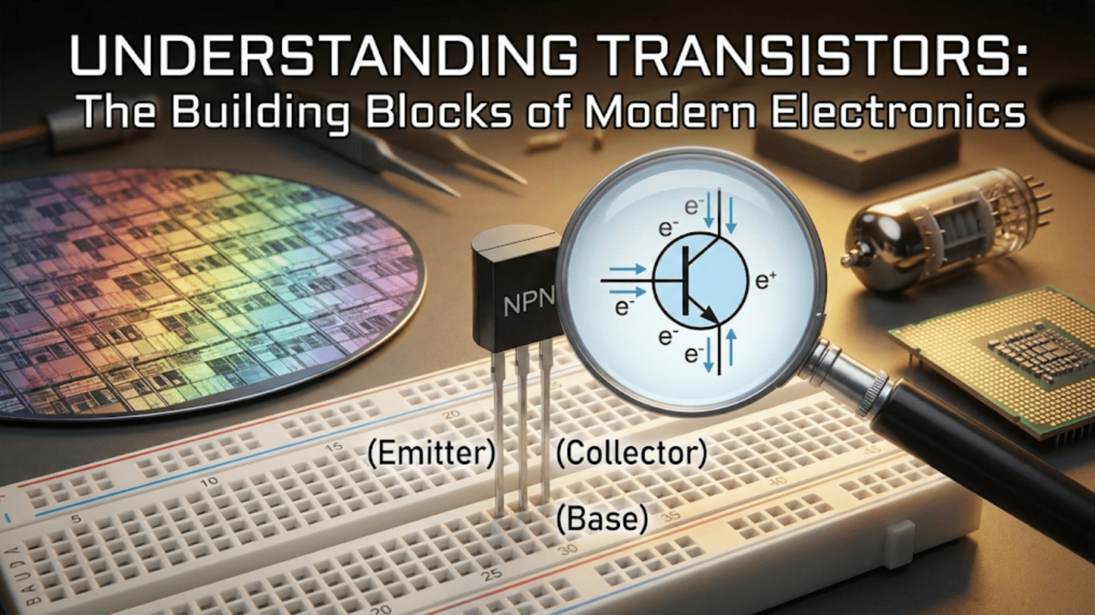
A transistor is a three-terminal semiconductor device that uses a small electrical signal at one terminal to control a much larger current between the other two terminals, functioning as either an amplifier (linearly controlling current) or a switch (fully on or fully off). The two main types are the BJT (Bipolar Junction Transistor), which is current-controlled, and the MOSFET (Metal-Oxide Semiconductor Field-Effect Transistor), which is voltage-controlled. Transistors are the fundamental building blocks of modern electronics: every integrated circuit, every processor, every smartphone contains billions of transistors acting as microscopic switches that represent the binary 0s and 1s of digital information.
Introduction: The Component That Changed Everything
In 1947, three physicists at Bell Laboratories—John Bardeen, Walter Brattain, and William Shockley—demonstrated a device they called a transistor. It was crude, fragile, and perplexing to understand, but it worked: a tiny voltage applied to one part of a semiconductor material controlled a much larger current flowing through another part. The transistor was awarded the Nobel Prize in Physics in 1956, and for good reason—it is arguably the most important invention of the 20th century.
Before transistors, electronics depended on vacuum tubes: glass bottles the size of light bulbs, requiring significant power to heat their filaments, fragile, expensive, and limited in how small they could be made. The first electronic computers—ENIAC and its contemporaries—filled entire rooms with thousands of tubes, consumed hundreds of kilowatts of power, and required constant maintenance as tubes failed. Transistors replaced tubes with a device smaller than a fingertip, requiring no warmup time, consuming far less power, and capable of switching billions of times per second.
But the transistor’s most transformative property wasn’t replacing individual vacuum tubes. It was that transistors could be made absurdly, almost incomprehensibly small—and that multiple transistors could be integrated onto a single piece of silicon. Today, a modern processor contains tens of billions of transistors in an area the size of a postage stamp. Each transistor is just a few nanometers across—smaller than many viruses. These microscopic switches, toggling between on and off states billions of times per second, are what create the computational power of the modern world.
Understanding transistors means understanding the foundation on which all modern electronics rests. Every microcontroller you program, every integrated circuit in your project, every logic gate in a digital circuit, every amplifier in an audio system—all of these are ultimately built from transistors. Understanding them moves you from electronics user to electronics creator: you can design circuits that control high-power loads from low-power signals, amplify weak sensor outputs to usable levels, interface different voltage domains, and build logic circuits from discrete components.
This comprehensive guide explores transistors from first principles through practical application. We’ll examine the semiconductor physics that makes transistors work, study the two dominant types (BJT and MOSFET) in depth, understand how transistors function as both amplifiers and switches, learn practical circuits using each type, and develop the intuition to use transistors confidently in your own designs.
Semiconductor Foundations: Why Transistors Work
The Nature of Semiconductors
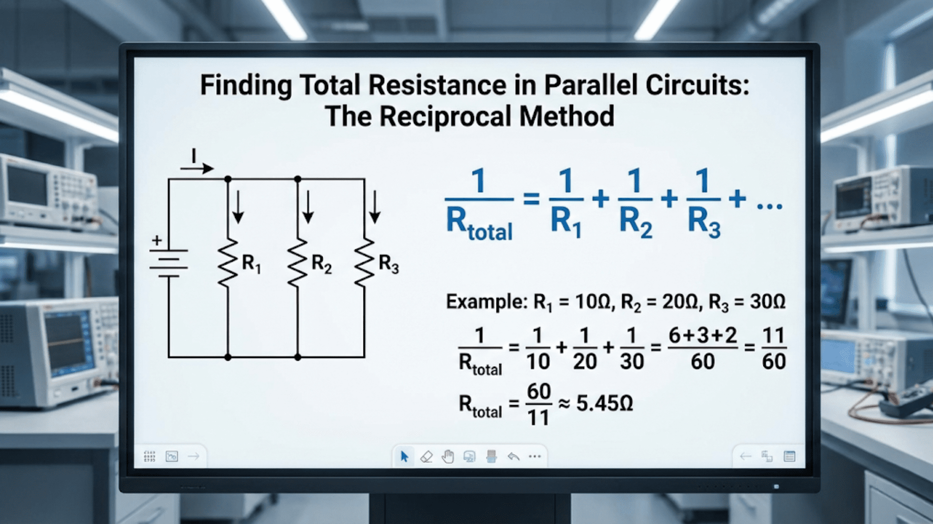
To understand transistors, you first need a basic picture of semiconductors—materials that conduct electricity, but not as well as metals, and whose conductivity can be controlled.
Pure silicon: A crystalline material where each silicon atom shares electrons with four neighboring atoms in a tight covalent bond lattice. At room temperature, very few electrons are free to conduct—pure silicon is a poor conductor.
Doped silicon — the key innovation:
Adding tiny amounts of impurities (“doping”) to pure silicon dramatically changes its electrical properties:
N-type silicon: Doping with phosphorus, arsenic, or antimony (elements with five outer electrons instead of silicon’s four) introduces extra electrons that are free to move. N-type silicon has an abundance of free negative charge carriers (electrons).
P-type silicon: Doping with boron, aluminum, or gallium (elements with three outer electrons) creates “holes”—positions where an electron is missing. Holes act as positive charge carriers and move through the crystal as electrons hop from hole to hole. P-type silicon has an abundance of free positive charge carriers (holes).
The P-N Junction: The Transistor’s Heart
When P-type and N-type silicon are joined, a P-N junction forms. This junction is the fundamental structure in all transistors and diodes.
At the junction: Free electrons from the N-side diffuse across the junction and recombine with holes on the P-side. This creates a “depletion region”—a zone depleted of free charge carriers, creating an electric field (built-in voltage) that opposes further diffusion.
Forward biasing (P positive, N negative): Applying voltage that opposes the built-in field collapses the depletion region, allowing current to flow. This is why a forward-biased diode conducts current.
Reverse biasing (P negative, N positive): Applying voltage in the same direction as the built-in field widens the depletion region, blocking current. A reverse-biased junction doesn’t conduct (until breakdown voltage is exceeded).
The transistor: Two P-N junctions arranged back-to-back with strategic doping create a device where one junction’s bias controls the current through both—the transistor.
BJT: Bipolar Junction Transistors
Structure and Terminals
A BJT consists of three semiconductor layers and two P-N junctions:
NPN transistor: N-type / P-type / N-type layers
- Base (B): The thin middle P-type layer—the control terminal
- Collector (C): One outer N-type layer—where most current enters
- Emitter (E): Other outer N-type layer—where current exits (heavily doped)
PNP transistor: P-type / N-type / P-type layers
- Base (B): The thin middle N-type layer—the control terminal
- Collector (C): One outer P-type layer
- Emitter (E): Other outer P-type layer (heavily doped)
NPN is more common and easier to use; this guide focuses on NPN with PNP discussed where differences are important.
How an NPN BJT Works
The physical mechanism:
- Without base current: The collector-base junction is reverse-biased. No current flows from collector to emitter. The transistor is OFF.
- With small base current: Forward-biasing the base-emitter junction injects electrons from the emitter into the thin base region. Most of these electrons don’t recombine with the base’s holes—instead, the electric field from the reverse-biased collector-base junction sweeps them across into the collector. A small base current therefore enables a large collector current.
- Current amplification: The ratio of collector current to base current is the current gain (β or hFE): β = I_C / I_B Typical β values: 50–500 (varies widely by transistor and operating point)
The three operating regions:
Cutoff region: Base current = 0 (or V_BE < ~0.6V). Collector current ≈ 0. Transistor OFF.
Active region: Base current present, transistor not saturated. I_C = β × I_B. Linear amplification possible. V_CE typically > 0.2–1V.
Saturation region: Base current provides more drive than needed for the collector current. Transistor fully ON. V_CE_sat ≈ 0.1–0.3V. I_C limited by the external circuit, not β.
Key BJT Equations
Current gain in active region: I_C = β × I_B
Kirchhoff’s current law at the transistor: I_E = I_C + I_B (Emitter current is the sum of collector and base currents)
Base-emitter voltage: V_BE ≈ 0.6–0.7V when forward-biased (similar to a diode forward voltage)
Collector-emitter saturation voltage: V_CE_sat ≈ 0.1–0.3V (transistor fully ON)
BJT as a Switch: Practical Circuit
NPN switch circuit:
VCC (12V)
    |
  [Load]     (e.g., 100Ω LED + resistor, motor, relay coil)
    |
Collector (C)
   [NPN BJT: 2N2222]
Emitter (E)
    |
   GND

Base (B) ----[R_base]---- Control Signal (from MCU, 5V GPIO)
Design procedure for saturation switch:
Step 1: Determine collector current I_C = (VCC – V_load) / R_load = (12V – 2V) / 100Ω = 100mA
Step 2: Calculate base current for saturation To guarantee saturation, drive 5–10× more base current than the minimum needed: I_B_min = I_C / β = 100mA / 100 = 1mA (using β = 100 typical) I_B_drive = 10 × I_B_min = 10mA (10× overdrive for reliable saturation)
Step 3: Calculate base resistor V_GPIO = 5V, V_BE = 0.7V R_base = (V_GPIO – V_BE) / I_B_drive = (5V – 0.7V) / 10mA = 430Ω → Use 470Ω
Step 4: Verify I_B = (5V – 0.7V) / 470Ω = 9.1mA (close enough to target) I_C_max = β × I_B = 100 × 9.1mA = 910mA >> 100mA → transistor saturates ✓
BJT as an Amplifier
In the active region (not saturated), BJT acts as a linear current amplifier:
Common emitter amplifier:
VCC
 |
[RC]  (collector resistor)
 |
Collector
[NPN BJT]
Emitter
 |
[RE]  (emitter resistor for stability)
 |
GND

Base ----[R1]---- VCC  (bias divider)
Base ----[R2]---- GND
Base ----[Cin]---- Input SignalVoltage gain (approximate): A_v ≈ -RC / re
Where re = 26mV / I_C (dynamic emitter resistance at room temperature)
Example: I_C = 1mA, RC = 10kΩ re = 26mV / 1mA = 26Ω A_v ≈ -10,000 / 26 ≈ -385
A small AC signal at the base produces a ~385× larger (inverted) signal at the collector. This is signal amplification.
Common BJT Types
Small-signal NPN:
- 2N2222 / PN2222A: Classic general-purpose, 600mA, 40V, β 100–300
- BC547 / BC548: European general-purpose, 100mA, 45V
- 2N3904: Popular general-purpose, 200mA, 40V
Small-signal PNP:
- 2N2907: PNP complement to 2N2222
- BC557: PNP complement to BC547
- 2N3906: PNP complement to 2N3904
Power NPN:
- TIP31, TIP41: Medium power, 3–6A, 60–100V
- 2N3055: Classic power transistor, 15A, 60V
- BD139: Small power, 1.5A, 80V
MOSFET: Metal-Oxide Semiconductor Field-Effect Transistors
Why MOSFETs Dominate Modern Electronics
While BJTs were the first transistors and remain important in analog circuits and high-frequency applications, MOSFETs dominate modern electronics for compelling reasons:
- Voltage-controlled: Gate draws virtually no current (extremely high input impedance). BJTs require base current continuously; MOSFETs only require charge to switch the gate capacitance.
- Lower on-resistance: Power MOSFETs can achieve on-resistance (R_DS_on) of milliohms, far lower than equivalent BJTs
- Faster switching: CMOS logic MOSFETs switch in picoseconds; ideal for digital circuits
- Scalability: MOSFETs can be made far smaller than BJTs; all modern processors use CMOS (Complementary MOSFET) technology
- Easy to drive: Logic-level gate voltage directly drives the gate; no current required in steady state
MOSFET Structure and Terminals
Terminals:
- Gate (G): Control terminal — applies voltage to control channel
- Drain (D): Where current enters (N-channel) or exits (P-channel)
- Source (S): Where current exits (N-channel) or enters (P-channel)
The gate is electrically isolated from the channel by a thin oxide layer (silicon dioxide). No DC current flows into the gate. This is why MOSFETs are voltage-controlled and why they draw near-zero quiescent current in digital CMOS logic.
N-Channel Enhancement MOSFET Operation
The most common MOSFET type for switching applications:
Structure: P-type substrate with two N-type regions (source and drain). A metal gate sits above the channel region, separated by the thin oxide.
Operation:
V_GS < V_th (threshold voltage): No channel forms between source and drain. No current flows. MOSFET is OFF. (Depletion region beneath gate has no free electrons.)
V_GS > V_th: The gate’s positive voltage attracts electrons from the P-type substrate to the surface, forming an N-type channel between source and drain. Current can now flow. MOSFET is ON.
V_GS >> V_th (fully enhanced): Channel is wide and conductive. R_DS_on (drain-source resistance when fully on) is minimized.
Key difference from BJT: The gate voltage creates/destroys the channel electrically. No gate current flows in steady state—only when the gate capacitance charges or discharges during switching. This makes MOSFET drive circuits far simpler than BJT base drive circuits for most applications.
MOSFET Key Parameters
V_th (Threshold Voltage): Gate voltage required to begin forming the channel. Typically 1–4V for standard MOSFETs; 0.5–2V for logic-level MOSFETs.
Logic-level vs. standard MOSFETs:
- Standard MOSFET: V_th = 2–4V, fully on at V_GS = 10V. Requires 10V gate drive — not directly compatible with 3.3V or 5V logic.
- Logic-level MOSFET: V_th = 0.5–2V, fully on at V_GS = 5V (often 3.3V). Directly compatible with microcontroller GPIO outputs.
When driving MOSFETs from a microcontroller, always choose logic-level MOSFETs unless a dedicated gate driver IC provides the required gate voltage.
R_DS_on (Drain-Source Resistance when ON): The resistance of the channel when fully enhanced. Determines conduction losses: P_loss = I_D² × R_DS_on
For low-power switching: R_DS_on = 0.1–10Ω acceptable For high-power switching: R_DS_on = milliohms preferred
V_DS_max (Drain-Source Voltage Maximum): Maximum voltage the MOSFET can block when OFF. Must be greater than VCC.
I_D_max (Drain Current Maximum): Maximum continuous current. Must exceed application current with margin.
Body diode: Every MOSFET has an internal diode between drain and source (formed by the MOSFET structure). This diode conducts in the reverse direction—important for inductive loads and H-bridge circuits.
MOSFET as a Switch: Practical Circuit
N-channel low-side switch:
VCC
 |
[Load]   (motor, LED strip, solenoid)
 |
Drain (D)
[N-channel MOSFET: IRLZ44N or 2N7000]
Source (S)
 |
GND

Gate (G) ----[R_gate 100Ω]---- MCU GPIO (3.3V or 5V)
Gate (G) ----[R_pulldown 100kΩ]---- GNDDesign notes:
- R_gate (100Ω): Limits gate charging current, reduces high-frequency ringing
- R_pulldown (100kΩ): Holds gate LOW when MCU is not driving it (prevents floating gate from turning MOSFET on unexpectedly)
- Choose MOSFET with V_th < 2V for 3.3V logic, V_th < 3V for 5V logic
- Verify R_DS_on at expected V_GS (datasheet gives curves)
N-channel high-side switch: High-side switching (load between MOSFET and VCC) with N-channel MOSFET requires gate voltage higher than VCC — needs gate driver or charge pump. P-channel MOSFET is easier for high-side switching when gate drive is simpler.
P-channel high-side switch:
VCC
 |
Source (S)
[P-channel MOSFET: IRF9540]
Drain (D)
 |
[Load]
 |
GND

Gate (G) ----[R_gate 100Ω]---- MCU GPIO (through inverter or level shifter)
Gate (G) ----[R_pullup 100kΩ]---- VCC (pull-up holds P-channel OFF when gate = VCC)P-channel turns ON when gate is LOW (below source voltage minus |V_th|). Turns OFF when gate is HIGH (at or above source voltage).
MOSFET in Power Applications
MOSFETs excel in power switching applications:
DC motor control: PWM (Pulse Width Modulation) to MOSFET gate controls average voltage to motor:
- Gate driven at 0: MOSFET off, motor stops
- Gate driven at 100%: MOSFET fully on, full speed
- Gate driven at 50%: Motor runs at ~50% speed
LED dimming: Same PWM principle for LED brightness control.
Switch-mode power supplies: MOSFETs switch at high frequency (50kHz–1MHz+) to efficiently convert voltages. The key metrics are low R_DS_on (reduces conduction losses) and fast switching (reduces switching losses).
H-bridge motor control: Four MOSFETs in an H-configuration allow current through a motor in both directions:
- Q1+Q4 on: Motor runs forward
- Q2+Q3 on: Motor runs reverse
- All off: Motor coasts
- Q1+Q2 on or Q3+Q4 on: NEVER (this shorts VCC to GND — shoot-through)
Common MOSFET Types
Logic-level N-channel (for MCU direct drive):
- 2N7000: Small signal, 200mA, 60V, V_th 0.8–3V — TO-92 package
- IRLZ44N: Power, 47A, 55V, R_DS_on 22mΩ — TO-220 package
- IRL540N: Power, 36A, 100V, R_DS_on 44mΩ — TO-220 package
- Si2302: Logic-level SOT-23, 2A, 20V — for SMD designs
Standard N-channel (need gate driver or 10V drive):
- IRF540: 28A, 100V, R_DS_on 77mΩ
- IRF3205: 110A, 55V, R_DS_on 8mΩ — for high current
Logic-level P-channel:
- IRF9Z34N: -19A, -55V — for high-side switching
- FDS9435: -5A, -20V, SOT-23 — SMD high-side switch
BJT vs. MOSFET: Choosing the Right Type
When to Use a BJT
High-frequency analog applications: BJTs have better high-frequency noise performance than MOSFETs in many analog circuits. RF amplifiers, audio circuits, and precision analog designs often prefer BJTs.
Precise current control: BJTs operating in their active region provide predictable current gain, making them useful where controlled current (not just on/off switching) is needed.
Low-voltage operation: BJTs can work at lower supply voltages than MOSFETs (which need V_GS > V_th to turn on). Some battery-powered analog circuits benefit from BJT characteristics at 1–2V supplies.
When driving cost is paramount: A BJT base can be driven by almost any small resistor from almost any logic signal. MOSFET gate drivers add cost in high-frequency switching applications.
Availability of complementary pairs: BJT NPN/PNP complementary pairs are well-characterized and widely available in matched specifications.
When to Use a MOSFET
Power switching: MOSFETs are almost always preferred for power switching due to lower R_DS_on, lower gate drive power, and better thermal performance.
High-frequency switching (power): At high switching frequencies (>100kHz), BJTs suffer from storage time issues during turn-off. MOSFETs switch faster with proper gate drive.
Digital logic and microprocessor circuits: CMOS (Complementary MOSFET) dominates all modern digital logic because of near-zero quiescent current consumption.
Direct GPIO drive: Logic-level MOSFETs can be driven directly from 3.3V or 5V GPIO pins; BJTs require careful base resistor calculation.
Battery and low-power applications: CMOS circuits consume power only during switching transitions, not in steady state—crucial for battery longevity.
Transistors in Integrated Circuits
How Transistors Form Logic Gates
The most profound application of transistors is in digital logic. CMOS technology uses pairs of complementary N-channel and P-channel MOSFETs to create logic gates that consume near-zero static power.
CMOS Inverter (NOT gate):
VDD (positive supply)
    |
   [P-MOSFET]
    |
    +-----> Output
    |
   [N-MOSFET]
    |
   GND

Input --> Both gatesOperation:
- Input = 0 (LOW): P-MOSFET ON (gate low, threshold exceeded), N-MOSFET OFF → Output connected to VDD → Output = 1 (HIGH)
- Input = 1 (HIGH): P-MOSFET OFF, N-MOSFET ON (gate high, channel forms) → Output connected to GND → Output = 0 (LOW)
The inverter uses only two transistors and draws significant current only during the brief switching moment, not in steady state.
NAND gate: Four transistors (two series N-channel, two parallel P-channel) NOR gate: Four transistors (two parallel N-channel, two series P-channel)
All of Boolean logic—AND, OR, NOT, XOR, XNOR—can be built from NAND or NOR gates, which are built from just 4 transistors each. The entire digital world emerges from this foundation.
Moore’s Law: Transistor Density Over Time
Moore’s Law (Gordon Moore, 1965): The number of transistors on an integrated circuit doubles approximately every two years.
Transistor counts in historical perspective:
- Intel 4004 (1971): 2,300 transistors
- Intel 8086 (1978): 29,000 transistors
- Intel 486 (1989): 1.2 million transistors
- Intel Pentium 4 (2004): 125 million transistors
- Apple M1 (2020): 16 billion transistors
- Apple M2 Ultra (2023): 134 billion transistors
Each transistor in a modern processor is roughly 3–5 nanometers in its key dimension—dozens of times smaller than a virus.
Why This Matters for Hobbyists
Understanding that the microcontroller in your Arduino project contains millions of transistors—each one of which operates on the same principles as the discrete transistors you can buy for pennies—transforms how you think about integrated circuits.
An ATmega328P (Arduino Uno’s MCU) contains roughly 130,000 transistors. These transistors form:
- The arithmetic logic unit (adds, subtracts, compares)
- The program memory (Flash, 32KB)
- The data memory (SRAM, 2KB)
- GPIO registers and drivers
- Timer/counter circuits
- ADC (analog-to-digital converter)
- UART, SPI, I²C communication hardware
Every one of those functions is ultimately built from the same transistor principles discussed in this article.
Practical Transistor Design Tips
Protecting Transistors with Inductive Loads
When switching inductive loads (motors, relays, solenoids), the inductor’s energy creates a voltage spike when the transistor turns off—potentially many times the supply voltage.
The danger: This spike appears across the transistor as a large V_CE or V_DS—far exceeding the transistor’s voltage rating. Result: immediate transistor destruction.
The solution: Flyback diode (freewheeling diode)
VCC
 |
[Inductive Load]
 |
+--[Diode: cathode to VCC, anode to collector/drain]
 |
Collector/Drain
[Transistor]
Emitter/Source
 |
GNDWhen the transistor switches off, the inductor drives the collector/drain voltage upward. The diode clamps it to VCC + one diode drop (~0.7V), safely diverting the inductive energy.
Diode selection:
- Rectifier diode (1N4007): Works for slow switching (motors, relays)
- Fast recovery or Schottky diode: Required for high-frequency PWM switching (normal rectifier diodes too slow)
Thermal Management
Transistors dissipate power: P_dissipation = V_CE × I_C (BJT in active region) P_dissipation = I_D² × R_DS_on (MOSFET in saturation)
As temperature rises, transistor characteristics change (BJT gain changes; MOSFET V_th decreases) and junction temperature may exceed maximum rating (typically 150–175°C) — causing permanent damage.
Thermal resistance: Each transistor package has a thermal resistance (θ_JA for junction-to-ambient): T_junction = T_ambient + P_dissipation × θ_JA
Example: TO-92 transistor: θ_JA ≈ 200°C/W 1W dissipation at 25°C ambient: T_junction = 25 + 1W × 200 = 225°C — EXCEEDS 150°C MAXIMUM!
Solution: Reduce power dissipation, use larger package (TO-220 has θ_JA ≈ 50°C/W), or add external heatsink.
The Gate Resistor for MOSFETs
Always include a gate resistor (typically 10–100Ω) between the drive source and MOSFET gate:
Why: The MOSFET gate is a capacitor. Driving it without resistance creates near-infinite instantaneous current spikes from the driver, causes ringing on the gate (which can cause the MOSFET to partially switch multiple times), and creates electromagnetic interference.
A small gate resistor damps the ringing while only slightly slowing switching speed.
Practical values:
- 10Ω: Fast switching with moderate damping
- 47Ω: Good compromise
- 100Ω: Slower switching, better damping (good for MCU direct drive)
- Higher values: Very slow switching (may increase switching losses in power applications)
Comparison Table: BJT vs. MOSFET
| Characteristic | BJT (NPN/PNP) | MOSFET (N/P-channel Enhancement) |
|---|---|---|
| Control type | Current-controlled (I_B controls I_C) | Voltage-controlled (V_GS controls I_D) |
| Input impedance | Low–moderate (base draws current) | Very high (gate is capacitive, near-infinite DC) |
| Drive requirement | Continuous base current in active region | Charge/discharge gate capacitance only |
| Threshold | V_BE ≈ 0.6–0.7V to turn on | V_GS > V_th (1–4V typically) |
| Current gain | β = 50–500 (hFE, varies widely) | Transconductance gm (not β) |
| Saturation voltage | V_CE_sat ≈ 0.2–1V | V_DS_on = I_D × R_DS_on (can be millivolts) |
| High-frequency analog | Excellent | Good but noisier (flicker noise) |
| Power switching | Good (Darlington for high current) | Excellent (low R_DS_on, fast) |
| Digital logic | Bipolar logic (ECL, TTL, now rare) | CMOS — universal standard |
| Static power (logic) | High (current in steady state) | Near-zero (only during switching) |
| Switching speed | Moderate (minority carrier storage) | Very fast (majority carrier only) |
| Complexity of drive | Simple (resistor + current) | Moderate (gate driver for high-speed) |
| Thermal runaway risk | Yes — positive feedback | Less so — R_DS_on increases with T |
| Body diode | No inherent body diode | Yes — integral body diode |
| Cost (discrete) | Very low | Low to moderate |
| Best applications | Audio amps, RF, precision analog, small switches | Power switching, digital logic, motor drive |
Conclusion: The Transistor Legacy
The transistor is simultaneously the simplest building block—a three-terminal device that controls current with a signal—and the most complex manufactured object humanity has ever created, with billions of instances packed into a cubic centimeter of silicon. Understanding both the simple principles and their profound implications is what electronics education makes possible.
What You Now Understand
The semiconductor physics: N-type and P-type silicon, P-N junctions, and how combining them creates current-controlling structures.
BJT operation: Base current controls collector current through current gain (β). Three regions: cutoff (off), active (amplifying), saturation (fully on). NPN for low-side switching, PNP less commonly for high-side.
MOSFET operation: Gate voltage creates or destroys a conducting channel. Voltage-controlled, near-zero gate current, logic-level types directly compatible with microcontrollers.
Switch vs. amplifier: Transistors in saturation/cutoff act as switches; transistors in the active/linear region act as amplifiers. The same device can serve both functions depending on biasing.
Practical applications: LED driving, motor control, relay switching, signal amplification, digital logic gates—all built on the same transistor principles.
Protection and reliability: Flyback diodes for inductive loads, gate resistors for MOSFETs, thermal management for power applications.
The Path Forward
Understanding discrete transistors opens the door to:
- Designing amplifier circuits — audio preamplifiers, sensor signal conditioning, instrumentation amplifiers
- Power electronics — motor drives, switching power supplies, battery chargers
- Digital logic design — understanding how gates work from first principles
- Understanding ICs — every op-amp, voltage regulator, microcontroller, and logic gate is built from transistors you now understand
The transistor is not just a component you use—it’s the vocabulary of electronics. Once you understand it deeply, all of modern electronics becomes readable, designable, and yours to create.
From John Bardeen’s crude germanium device in 1947 to the 3-nanometer silicon transistors in today’s processors, the fundamental principle has never changed: a small electrical signal controls a much larger one. Everything else—the entire digital revolution, the smartphone, the internet, artificial intelligence—flows from that single, elegant idea.