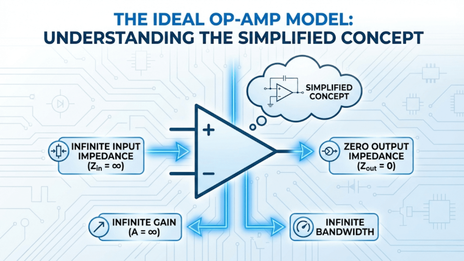
The ideal op-amp model is a simplified analytical framework that treats an operational amplifier as having infinite open-loop gain, infinite input impedance, zero output impedance, infinite bandwidth, and zero input offset voltage. These idealizations make op-amp circuit analysis straightforward and produce results accurate to within 1% for most real-world circuits, because negative feedback makes circuit behavior depend on external passive components rather than the op-amp’s internal characteristics.
Introduction: The Power of Useful Simplification
Every field of engineering relies on simplified models. Physicists treat planets as point masses to calculate orbits. Structural engineers assume steel behaves linearly under normal loads. Chemical engineers use ideal gas laws for preliminary process design. These simplifications are not mistakes — they are deliberate choices to make complex systems tractable while retaining enough accuracy for practical use.
Electronics is no different. Real transistors have dozens of parameters that vary with temperature, current, frequency, and manufacturing tolerances. Real capacitors have parasitic inductance and resistance. Real resistors have temperature coefficients and noise. If every circuit analysis had to account for every non-ideal parameter, electronics design would be impossibly complex.
The ideal op-amp model is one of electronics’ most useful and elegant simplifications. By assuming five idealized properties, it reduces what would otherwise be a complex analysis involving 20 transistors and their interactions to a simple application of two rules — rules so straightforward that a beginner can use them correctly within minutes of learning them.
But the ideal model’s value goes beyond convenience. Because op-amps are used with negative feedback, the actual performance of a well-designed op-amp circuit is genuinely close to what the ideal model predicts — often within 0.1% for DC circuits using readily available components. The simplification works because negative feedback suppresses the effects of the very non-idealities the model ignores.
This article takes the ideal op-amp model seriously as an intellectual object worth understanding deeply. We’ll examine each of the five idealizations in detail — what they mean mathematically, what they enable analytically, and how far real op-amps deviate from each ideal. We’ll develop the two golden rules from first principles, explore the virtual ground and virtual short concepts that flow from those rules, work through multiple circuit analyses using the model, and examine where the ideal model breaks down and what that means for practical design.
By the end of this article, you’ll not just know the golden rules — you’ll understand why they work, when to apply them with confidence, and when to look beyond the ideal model to real-world op-amp behavior.
The Five Idealizations: A Deep Examination
Idealization 1: Infinite Open-Loop Gain (A_OL = ∞)
The open-loop gain is the gain of the amplifier with no external feedback applied — the raw amplification factor from differential input to output.
What it means mathematically:
V_out = A_OL × (V+ − V−)For an ideal op-amp, A_OL = ∞. This means that for any finite output voltage, the differential input (V+ − V−) must be:
(V+ − V−) = V_out / A_OL = V_out / ∞ = 0So with negative feedback maintaining a finite output, the differential input voltage is identically zero — the two inputs are forced to the same voltage. This is the mathematical basis for the second golden rule (virtual short).
What real op-amps have:
Typical DC open-loop gains range from 100,000 (100dB) to 10,000,000 (140dB) depending on the device. The classic µA741 has A_OL ≈ 200,000 (106dB). Precision op-amps like the OP07 achieve A_OL ≈ 1,000,000 (120dB). These are enormous numbers — so large that for virtually all closed-loop circuit analysis, treating them as infinite introduces negligible error.
The error introduced by finite gain:
For a closed-loop gain G_CL set by external resistors, the actual closed-loop gain with finite open-loop gain A_OL is:
G_actual = A_OL × G_CL / (A_OL + G_CL) ≈ G_CL × (1 − G_CL/A_OL)For A_OL = 200,000 and G_CL = 100 (a gain-100 amplifier):
Error = G_CL / A_OL = 100 / 200,000 = 0.05%The actual gain is 0.05% below the ideal. For a 1% resistor, this error is completely negligible. The ideal approximation is excellent.
When finite gain matters:
The finite gain assumption fails when the desired closed-loop gain approaches A_OL itself — which would require you to run an op-amp at near-unity feedback or with an extremely high gain stage. In practice, op-amps are almost never used at gains approaching A_OL, so this is rarely a concern in normal circuit design.
It also matters at higher frequencies, where the op-amp’s open-loop gain drops dramatically. At 10kHz, a 741 might have only A_OL ≈ 100, making the ideal assumption much less accurate at audio frequencies when high gain is required.
Idealization 2: Infinite Input Impedance (Z_in = ∞)
The input impedance is the impedance seen looking into either input terminal — the effective load the op-amp presents to whatever drives its inputs.
What it means:
Infinite input impedance means zero current flows into either input terminal under any conditions:
I+ = 0    (no current into non-inverting input)
I− = 0 (no current into inverting input)This is the first golden rule, stated directly. Because no current enters the input terminals, the Kirchhoff’s Current Law (KCL) analysis at any node connected to an input is simplified — the op-amp input draws no current from that node.
What real op-amps have:
Input impedance depends on the op-amp’s input stage technology:
| Input Stage Type | Typical Input Impedance | Typical Bias Current | Example Op-Amps |
|---|---|---|---|
| BJT differential pair | 1MΩ – 10MΩ | 10nA – 500nA | µA741, LM741, NE5532 |
| Darlington BJT pair | 10MΩ – 100MΩ | 1nA – 50nA | LM318 |
| JFET differential pair | 10¹² Ω (1TΩ) | 1pA – 50pA | TL071, TL081, LF356 |
| MOSFET differential pair | 10¹³ Ω+ | 0.001pA – 1pA | LMC6001, AD8622 |
BJT inputs draw tens to hundreds of nanoamps (input bias current). JFET and MOSFET inputs draw picoamps — effectively zero for most purposes.
The error introduced by finite input impedance:
Finite input impedance matters when the source resistance driving the op-amp input is a significant fraction of the input impedance. Consider driving a BJT op-amp (Z_in = 2MΩ) from a 100kΩ source:
The source and input impedance form a voltage divider:
V_actual = V_source × Z_in / (Z_source + Z_in) = V_source × 2M / (100k + 2M) = 0.952 × V_sourceA 4.8% error — significant for precision work. Solution: use a JFET-input op-amp (TL071, Z_in ≈ 10¹²Ω) or a voltage follower buffer stage before the high-source-impedance node.
Bias current errors:
The more practical consequence of finite input impedance for BJT op-amps is not the impedance loading but the input bias current. Even a small bias current creates a voltage error when flowing through resistance. For a 741 with I_B = 80nA driving a 100kΩ feedback resistor:
V_error = I_B × R_f = 80×10⁻⁹ × 100,000 = 8mVFor a gain-100 amplifier, this 8mV input error appears as 800mV at the output — a significant DC error. This is why BJT op-amps need bias current compensation, and why JFET op-amps are preferred for high-impedance applications.
Idealization 3: Zero Output Impedance (Z_out = 0)
Zero output impedance means the op-amp output is a perfect voltage source: it delivers whatever current is needed to maintain the output voltage regardless of the load.
What it means:
V_out_loaded = V_out_unloaded (for any load current)No matter how much current the load demands, the output voltage doesn’t change. This makes analysis simple: you can calculate V_out from the circuit equations and apply it to any load without worrying about voltage division between Z_out and Z_load.
What real op-amps have:
Open-loop output impedance for a typical op-amp is 50Ω to 200Ω. This might seem significant, but with negative feedback, the effective closed-loop output impedance drops dramatically:
Z_out_closed = Z_out_open / (1 + A_OL × β)Where β is the feedback fraction (the fraction of output fed back to the inverting input). For a gain-10 inverting amplifier (β ≈ 0.1) with 741 (A_OL = 200,000, Z_out_open = 75Ω):
Z_out_closed = 75 / (1 + 200,000 × 0.1) = 75 / 20,001 ≈ 0.00375ΩLess than 4 milliohms! The feedback mechanism reduces the output impedance by the same factor it reduces sensitivity to open-loop gain variations. This is why the ideal assumption of zero output impedance is so accurate in practice — feedback does all the work.
When output impedance matters:
Real op-amps have output current limits — typically 10mA to 25mA for general-purpose types. If the load demands more current than this, the output voltage will drop (the op-amp clips). A 741 trying to drive a 100Ω load from a ±15V supply would need to source 150mA — far beyond its capability. The output will clip long before reaching the rail.
The output impedance model breaks down not from the impedance value itself, but from the current limiting. Solutions: buffer the output with a transistor or emitter follower, use a high-current op-amp (OPA548, LM675), or use a power op-amp designed for heavy loads.
Idealization 4: Infinite Bandwidth (BW = ∞)
Infinite bandwidth means the op-amp amplifies all frequencies equally, from DC to infinitely high frequencies, with no phase shift.
What it means:
The open-loop gain A_OL is constant at all frequencies:
|A_OL(f)| = A_OL(DC) for all fNo frequency-dependent rolloff, no phase shift.
What real op-amps have:
This is where the ideal model deviates most significantly from reality. Real op-amps are intentionally designed with a frequency-dependent gain rolloff, typically beginning at a very low frequency (often just 1Hz to 10Hz for the open-loop −3dB frequency) and rolling off at 20dB per decade (−6dB per octave).
The open-loop gain of a compensated op-amp follows:
A_OL(f) ≈ A_OL(DC) / (1 + j×f/f_c)Where f_c is the dominant pole frequency (often just a few hertz). This makes the open-loop gain fall with frequency, crossing 0dB (unity gain) at the gain-bandwidth product (GBW) frequency.
For a 741 with A_OL(DC) = 200,000 and GBW = 1MHz:
- At f = 10Hz: A_OL ≈ 200,000 (essentially DC value)
- At f = 1kHz: A_OL ≈ 1,000
- At f = 10kHz: A_OL ≈ 100
- At f = 100kHz: A_OL ≈ 10
- At f = 1MHz: A_OL ≈ 1 (unity gain bandwidth)
The gain-bandwidth product rule:
For a single-pole compensated op-amp, the closed-loop gain and bandwidth are related:
G_CL × f_−3dB = GBWThe product of closed-loop gain and −3dB bandwidth is constant and equals the unity-gain bandwidth. This means higher gain gives lower bandwidth:
- Gain 1 (voltage follower): bandwidth = GBW = 1MHz (for 741)
- Gain 10: bandwidth = 100kHz
- Gain 100: bandwidth = 10kHz
- Gain 1000: bandwidth = 1kHz
For audio amplification of 20Hz–20kHz at gain 100, the 741’s 10kHz bandwidth is just barely adequate for the lower half of the audio spectrum but rolls off through the upper half — poor for high-fidelity audio. An op-amp like the NE5532 (GBW = 10MHz) with gain 100 gives 100kHz bandwidth — more than adequate for audio.
Why frequency compensation is intentional:
Op-amps are deliberately compensated (gain rolled off) to prevent oscillation. Without compensation, the multiple internal poles (each contributing −90° phase shift) would accumulate enough phase shift that the feedback loop becomes positive at some frequency, causing the circuit to oscillate. The dominant pole compensation ensures the phase shift reaches −180° only after the gain has dropped below unity, preventing oscillation. This is called “phase margin.”
Idealization 5: Zero Input Offset Voltage (V_OS = 0)
An ideal op-amp outputs exactly 0V when both inputs are at exactly the same voltage. Any circuit powered by an ideal op-amp with both inputs grounded will have zero output.
What real op-amps have:
Real op-amps have a small but nonzero output voltage even with identical inputs, due to manufacturing mismatches in the differential pair transistors. This is expressed as the equivalent input offset voltage V_OS — the small differential input voltage that would be needed to bring the output to exactly zero.
Typical values:
- µA741: V_OS = 1–6mV typical, 6mV maximum at 25°C
- TL071: V_OS = 3–15mV typical
- OP07: V_OS = 25–75µV (precision grade)
- AD8628: V_OS = 1–5µV (auto-zero, ultra-precision)
The effect of offset voltage on circuit output:
For an inverting or non-inverting amplifier with closed-loop gain G_CL, the output error due to V_OS is:
V_out_error = V_OS × G_CLFor a 741 (V_OS = 2mV typical) at gain 100:
V_out_error = 2mV × 100 = 200mVA 200mV DC offset at the output — clearly visible and potentially significant depending on the application. For audio (AC-coupled), this is usually irrelevant. For precision DC measurement, it represents a serious error that requires compensation.
Offset voltage compensation techniques:
Most precision op-amps include offset adjustment pins (null pins). For the 741, connecting a 10kΩ potentiometer between pins 1 and 5 with the wiper to the negative supply allows trimming the offset to zero. However, trimmed offset drifts with temperature, so trimming only helps for constant-temperature applications.
The better long-term solution is to choose a precision op-amp with inherently low offset (OP07, AD8628) or use an auto-zero (chopper-stabilized) op-amp that continuously nulls its own offset.
Offset drift:
Even after trimming, the offset voltage changes with temperature. The temperature coefficient of offset voltage (V_OS/°C, or offset drift) is typically 2–10µV/°C for standard op-amps and 0.01–0.05µV/°C for auto-zero types.
Deriving the Golden Rules from the Idealizations
With the five idealizations established, the two golden rules follow directly.
Deriving Golden Rule 1: No Current Flows into Either Input
From Idealization 2 (infinite input impedance):
Z_in = ∞ → I = V/Z_in = V/∞ = 0No voltage, however large, can drive current through an infinite impedance. Therefore, no current flows into either input terminal of an ideal op-amp.
This rule applies regardless of what voltages appear at the inputs. It is absolute within the ideal model.
Practical application: At any node connected to an op-amp input, you can write KCL ignoring the current flowing into the op-amp input. All currents at that node come from and go to external components only.
Deriving Golden Rule 2: With Negative Feedback, V+ = V−
This rule requires combining Idealization 1 (infinite gain) with the existence of negative feedback.
Step 1: The output voltage is:
V_out = A_OL × (V+ − V−)Step 2: For a finite output voltage with A_OL → ∞:
(V+ − V−) = V_out / A_OL → 0 as A_OL → ∞Step 3: Therefore, in any circuit where negative feedback keeps the output from saturating:
V+ − V− = 0 → V+ = V−The op-amp continuously adjusts its output to whatever value is needed to maintain V+ = V−. If V+ momentarily exceeds V−, the output increases (for a non-inverting configuration), which feeds back to increase V−, reducing the error. The system converges on V+ = V−.
Critical condition: This rule only applies when negative feedback is present and the op-amp is operating in its linear region (not saturated). In open-loop operation or when the output is clipped at a supply rail, V+ ≠ V− in general.
The “virtual short” name: The condition V+ = V− makes the two input terminals electrically equivalent in terms of voltage — like a short circuit between them. But no current flows between them (Rule 1 — infinite impedance). It’s a “virtual” short: same voltage, zero current. The virtual short is the analytical tool that makes op-amp circuit analysis tractable.
Systematic Circuit Analysis Using the Two Golden Rules
The golden rules provide a systematic procedure for analyzing any op-amp circuit with negative feedback. The procedure always follows the same steps.
The Standard Analysis Procedure
- Identify V+: Determine the voltage at the non-inverting input from the external circuit.
- Apply Rule 2: Set V− = V+ (virtual short — this is the key step).
- Apply Rule 1: Write KCL at the V− node, noting that no current flows into the op-amp input. All current at this node flows through external components only.
- Solve for V_out from the KCL equation.
This procedure works for inverting amplifier, non-inverting amplifier, summing amplifier, integrator, differentiator, and most other linear op-amp configurations. Let’s apply it systematically to three circuits.
Analysis Example 1: Inverting Amplifier
Circuit: R_in connects V_in to V−. R_f connects V_out to V−. V+ is connected to ground (0V).
Step 1: V+ = 0V (grounded)
Step 2: V− = V+ = 0V (virtual ground — the inverting input is a virtual ground)
Step 3: KCL at V− node. Current flowing into the node through R_in:
I_Rin = (V_in − V−) / R_in = (V_in − 0) / R_in = V_in / R_inCurrent flowing out of the node through R_f (toward V_out):
I_Rf = (V− − V_out) / R_f = (0 − V_out) / R_f = −V_out / R_fNo current into op-amp input (Rule 1), so:
I_Rin + I_Rf = 0   (KCL at virtual ground node)
V_in / R_in + (−V_out / R_f) = 0
V_in / R_in = V_out / R_fStep 4: Solving for V_out:
V_out = −(R_f / R_in) × V_inClosed-loop gain: G = −R_f / R_in
The negative sign confirms signal inversion. The gain magnitude is set purely by the resistor ratio — independent of the op-amp’s actual gain, input impedance, or output impedance (within the ideal model).
Analysis Example 2: Non-Inverting Amplifier
Circuit: V_in connects to V+. R_in connects V− to ground. R_f connects V_out to V−.
Step 1: V+ = V_in
Step 2: V− = V+ = V_in
Step 3: KCL at V− node. The voltage at V− is V_in (from virtual short). The external connections at V− are R_in (to ground) and R_f (to V_out). No current into op-amp (Rule 1).
Current through R_in (from V− to ground):
I_Rin = V− / R_in = V_in / R_in (flows from V− toward ground)Current through R_f (from V_out to V−):
I_Rf = (V_out − V−) / R_f = (V_out − V_in) / R_f (flows from V_out toward V−)KCL: current into node = current out of node:
(V_out − V_in) / R_f = V_in / R_in
V_out − V_in = V_in × R_f / R_in
V_out = V_in + V_in × R_f / R_in = V_in × (1 + R_f / R_in)Step 4: Closed-loop gain: G = 1 + R_f / R_in
Always ≥ 1. No phase inversion. Input impedance is very high (the op-amp input impedance, not set by R_in).
Analysis Example 3: Weighted Summing Amplifier
Circuit: V1 through R1, V2 through R2, V3 through R3, all to V−. R_f from V_out to V−. V+ to ground.
Step 1: V+ = 0V
Step 2: V− = 0V (virtual ground)
Step 3: KCL at virtual ground node. Three input currents and one feedback current, no current into op-amp:
I_R1 = V1 / R1   (into virtual ground node)
I_R2 = V2 / R2   (into virtual ground node)
I_R3 = V3 / R3   (into virtual ground node)
I_Rf = −V_out / R_f (out of virtual ground node, toward V_out)KCL:
V1/R1 + V2/R2 + V3/R3 = V_out/R_fStep 4:
V_out = −R_f × (V1/R1 + V2/R2 + V3/R3)If all input resistors are equal (R1 = R2 = R3 = R):
V_out = −(R_f / R) × (V1 + V2 + V3)The output is a scaled, inverted sum of all inputs. Each input contributes independently — changing V1 doesn’t affect the contributions of V2 or V3, because the virtual ground keeps the summing node at 0V regardless of other inputs.
This is the virtual ground’s most powerful property: it decouples the inputs in a summing amplifier, preventing interaction between channels.
Where the Ideal Model Breaks Down: A Practical Map
The ideal model is remarkably accurate under typical conditions, but understanding its failure modes helps you know when to look beyond it.
Failure Zone 1: High Frequencies
At frequencies approaching and exceeding f_c (the op-amp’s dominant pole, often just 10Hz for some devices), the open-loop gain drops significantly. The ideal model assumes A_OL = ∞, but:
- Closed-loop gain begins to fall below the ideal resistor-ratio value
- Phase shift accumulates, potentially causing stability issues
- The virtual short relationship (V+ = V−) degrades — there IS a small differential voltage at higher frequencies
When to abandon the ideal model for frequency analysis: When the signal frequency approaches GBW / G_CL (the closed-loop bandwidth). At this point, use the full frequency-domain model including the gain-bandwidth product.
Failure Zone 2: Large Output Swings at High Frequencies (Slew Rate)
The slew rate limitation is a nonlinear effect not captured by the linear ideal model. Even if the small-signal bandwidth is adequate, a fast-rising large-amplitude signal may be slew-rate limited — the output simply cannot change fast enough.
Maximum undistorted output frequency for a sinusoid:
f_max = Slew Rate / (2π × V_peak)For a 741 (SR = 0.5V/µs) with V_peak = 10V:
f_max = 500,000 / (2π × 10) = 7,958Hz ≈ 8kHzAbove 8kHz, the 741 output cannot swing ±10V as a clean sine wave — it produces a triangular wave instead. The ideal model predicts clean sinusoids; reality produces distorted triangles.
Failure Zone 3: Large Input Offset and Drift in Precision DC Circuits
For DC-coupled precision measurement circuits amplifying very small signals (microvolts to millivolts), the input offset voltage and its temperature drift become the dominant error sources. The ideal model ignores offset entirely.
Example: Measuring a 1mV thermocouple voltage with gain 1000. Ideal output: 1V. Real output with 1mV offset: 2V (100% error!). Choose a precision op-amp (OP07: V_OS = 25µV max → output error = 25mV, 2.5% error) or an auto-zero type (AD8628: V_OS = 5µV max → 0.5% error).
Failure Zone 4: High Source Impedance with BJT Input Op-Amps
When the signal source has high impedance (above ~100kΩ) and a BJT input op-amp is used, the input bias current creates significant voltage errors across the source resistance. The ideal model (zero input current) misses this entirely.
For a photodiode transimpedance amplifier with 10MΩ feedback resistor and 741 (I_B = 80nA):
V_error = I_B × R_f = 80nA × 10MΩ = 800mVThis completely overwhelms any small photodiode signal. Solution: use JFET input op-amp (TL071, I_B < 50pA → V_error < 0.5mV) or MOSFET input (even lower bias current).
Failure Zone 5: Output Loading Beyond Current Limits
The ideal model assumes zero output impedance — infinite current drive capability. Real op-amps have output current limits (typically 10–25mA). Loads requiring more current than this limit cause output voltage clipping even though the ideal model would predict normal operation.
For a 741 (I_out_max ≈ 25mA) driving a 200Ω load from 5V supply:
I_required = 5V / 200Ω = 25mA — right at the limitThe output will likely clip or distort. Use a buffer transistor or a power op-amp for heavy loads.
Real Op-Amp Parameters vs. Ideal: A Comprehensive Comparison
| Parameter | Ideal Value | Typical Real Value | Effect of Deviation |
|---|---|---|---|
| Open-loop gain (A_OL) | ∞ | 10⁵ – 10⁷ | Gain error < 0.001–0.1% at low gain |
| Input impedance (differential) | ∞ | 1MΩ – 10TΩ | Loading error for high Z sources |
| Input impedance (common-mode) | ∞ | 100MΩ – 1TΩ | Affects CMRR |
| Output impedance | 0 | 50Ω – 200Ω (open-loop) | Negligible with feedback (<1Ω) |
| Bandwidth | ∞ | GBW: 0.5MHz – 1GHz | Gain rolloff above f_c |
| Offset voltage | 0V | 1µV – 10mV | Output DC error = V_OS × G_CL |
| Offset drift | 0 | 0.01 – 10µV/°C | Temperature-dependent output error |
| Input bias current | 0 | 1fA – 500nA | Error across source resistance |
| CMRR | ∞ | 80–120dB | Amplification of common-mode noise |
| PSRR | ∞ | 80–120dB | Supply noise appears at output |
| Slew rate | ∞ | 0.1 – 6000 V/µs | Distortion at high frequency, large signal |
| Output current | ∞ | 10 – 100mA | Clipping with heavy loads |
The Ideal Model in Historical Context
It’s worth understanding why the ideal op-amp model was developed and why it remains the standard teaching approach.
In the 1940s and 1950s, analog computers used op-amps to perform mathematical operations — integration, differentiation, addition, subtraction — in solving differential equations. The designers discovered that with sufficiently high loop gain, the circuit’s behavior became dependent on stable, precision passive components (resistors and capacitors) rather than the variable, temperature-sensitive vacuum tubes implementing the amplifier.
This was a profound realization: high-gain feedback systems automatically correct for their own internal imperfections. The better the op-amp’s open-loop gain, the more accurately it performs the mathematical operation defined by the external components. The ideal model simply takes this observation to its logical limit — infinite gain means perfect operation defined entirely by external components.
The fact that this limit is so closely approached in practice (within 0.01–1% for most applications) is what makes the ideal model so powerful. It’s not just a pedagogical simplification — it’s an accurate description of how well-designed feedback systems actually behave.
Applying the Ideal Model: A Design Philosophy
Understanding the ideal model transforms how you approach op-amp circuit design. Rather than trying to understand the complex internal workings of 20 transistors, you work with the simple behavioral model:
Design the external network to define the desired mathematical relationship between input and output (using the golden rules to derive the transfer function).
Choose a real op-amp whose non-ideal characteristics are small enough not to matter for your application — adequate GBW for your frequency range, low enough offset for your precision requirements, sufficient output current for your load, appropriate input technology (BJT or FET) for your source impedance.
Verify the design by checking that your operating conditions fall well within the ideal model’s range of validity:
- Closed-loop gain << open-loop gain at your highest frequency
- Source impedances << op-amp input impedance (or account for bias current effects)
- Output swing stays within the supply rails and current limits
- Slew rate adequate for your signal amplitude and frequency
This three-step approach — design with ideal model, choose real device, verify validity — is the professional workflow for op-amp circuit design. It works because the ideal model captures the essential behavior of real op-amps operating in their intended conditions.
Summary
The ideal op-amp model’s five properties — infinite open-loop gain, infinite input impedance, zero output impedance, infinite bandwidth, and zero offset voltage — are not arbitrary simplifications. Each idealization is well-justified for real op-amps operating under typical conditions, and the errors introduced are generally less than 0.1% for common applications.
The two golden rules flow directly from these idealizations: no current into the inputs (from infinite input impedance), and negative feedback forces V+ = V− (from infinite open-loop gain). These rules enable systematic analysis of any negative-feedback op-amp circuit using straightforward KCL.
The virtual short concept — two inputs at the same voltage with zero current between them — is the analytical key that unlocks the inverting amplifier (virtual ground at the inverting input), non-inverting amplifier, summing amplifier, integrator, differentiator, and all other linear op-amp configurations.
The ideal model breaks down at high frequencies (gain-bandwidth product), with large rapid output swings (slew rate), in precision DC circuits (offset voltage), with high-impedance sources and BJT inputs (bias current), and with heavy output loads (current limiting). Recognizing these failure zones guides selection of the appropriate real op-amp for each application.
The ideal op-amp model is not a stepping stone to be abandoned once “real” op-amp behavior is learned — it is the correct design framework, with known, quantifiable corrections applied when specific application requirements demand them.