Using a transistor as a switch means driving it between two states: fully OFF (cutoff region, where base current is zero and no collector current flows) and fully ON (saturation region, where the transistor acts like a closed switch with only ~0.2V across it). The key design steps are calculating the collector current required by the load, determining the minimum base current needed for saturation (I_C ÷ β), applying a 5–10× overdrive factor for reliable saturation, and choosing a base resistor to deliver that current from the available control voltage. This fundamental circuit allows a 5V microcontroller GPIO pin outputting milliamps to control motors, relays, solenoids, and LED strips drawing amps.
Introduction: The Transistor’s Two Greatest Roles
Of everything a transistor can do, two applications dominate practical electronics: switching and amplification. These might seem like different concepts, but they’re actually two extremes of the same device — two different operating regions of the same three-terminal semiconductor. A transistor used as a switch spends its time either completely off or completely on, with nothing in between. A transistor used as an amplifier spends its time in the linear middle ground, where small input changes produce proportional larger output changes.
For most beginners, switching comes first and makes the most immediate practical impact. The moment you realize you can control a 12V motor drawing 2 amps using nothing but a microcontroller GPIO pin outputting 3.3V and a few milliamps is genuinely exciting. That tiny signal, through the transistor’s amplifying action, commands a load hundreds of times more powerful than the signal itself. This is the promise of transistor switching — it’s what makes microcontrollers useful in the physical world, connecting digital logic to real actuators, lights, and mechanisms.
Amplification opens a different door: the ability to take a weak signal — perhaps a few microvolts from a microphone capsule, a few millivolts from a thermocouple, or a hundredth of a volt from a sensor — and magnify it to a level that can be measured, processed, or transmitted. Without amplification, most sensors would be unusable, audio systems would be silent, and radio communication would be impossible. The transistor amplifier is the bridge between the microscopic world of physical signals and the practical world of circuits that can process them.
This article develops both skills through hands-on circuit design. We’ll start with transistor switching — working through the design process step by step, with real calculations and component values — then transition to amplifier design, building the foundational common-emitter amplifier that appears in textbooks, audio gear, radio transmitters, and sensor interfaces worldwide.
By the end, you’ll have the tools to design your own switching and amplification circuits from scratch, understand what each component does and why it’s there, and troubleshoot circuits that don’t behave as expected.
Part 1: The Transistor as a Switch
The Two Switching States
A transistor used as a switch operates exclusively in two regions:
Cutoff (OFF state):
- Base-emitter voltage V_BE < 0.6V (for silicon NPN)
- No base current flows: I_B = 0
- No collector current flows: I_C ≈ 0
- All the supply voltage appears across the transistor: V_CE ≈ VCC
- The transistor behaves like an open switch
Saturation (ON state):
- Sufficient base current forces the transistor fully ON
- Collector current limited by the external circuit (load), not by β
- Collector-emitter saturation voltage: V_CE_sat ≈ 0.1–0.3V (very small)
- The transistor behaves like a closed switch with a tiny voltage drop
The active region (avoid in switching applications): Between cutoff and saturation lies the active (linear) region where I_C = β × I_B. In this region, the transistor dissipates significant power (V_CE × I_C can be substantial) and doesn’t function cleanly as a switch. Good switching circuit design ensures the transistor spends as little time as possible in the active region — transitioning quickly through it.
The Basic NPN Switch Circuit
       VCC (+12V)
          │
        [Load]          ← e.g., relay coil (120Ω), motor, LED string
          │
          C (Collector)
    ┌────[NPN Q1]
    │     E (Emitter)
    │        │
    │       GND
    │
└── B (Base)──[R_base]──Control (MCU GPIO, 5V = ON)This is the fundamental low-side NPN switch. The load connects between VCC and the collector; the emitter connects to GND; the base is driven by the control signal through a current-limiting resistor.
Step-by-Step Switch Design: Complete Example
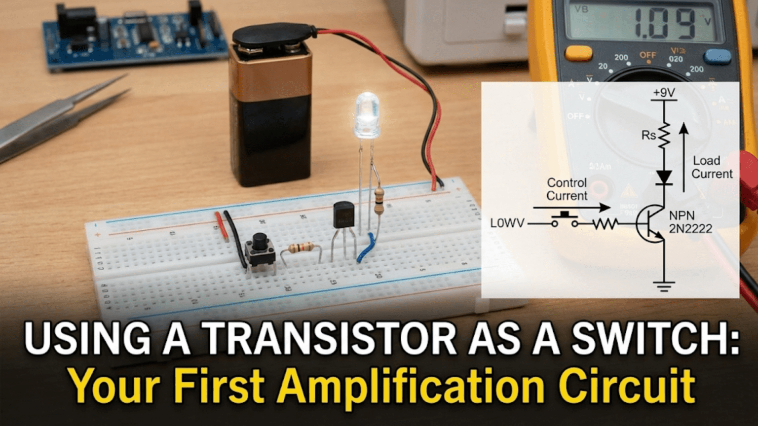
Design goal: Control a 12V relay coil (resistance = 120Ω) from a 5V Arduino GPIO pin, using a 2N2222 NPN transistor.
Step 1: Determine the required collector current
The relay coil draws: I_C = VCC / R_coil = 12V / 120Ω = 100mA
Step 2: Find transistor β (current gain)
From the 2N2222 datasheet:
- hFE (β) at I_C = 100mA, V_CE = 10V: minimum 35, typical 100
Always design for the minimum β to guarantee the circuit works with any transistor from the batch. β_min = 35
Step 3: Calculate minimum base current for saturation
At minimum β, the transistor just saturates when: I_B_min = I_C / β_min = 100mA / 35 = 2.86mA
Step 4: Apply overdrive factor
For reliable saturation (accounting for β variation, temperature effects, component tolerances), use 5–10× overdrive: I_B_target = 5 × I_B_min = 5 × 2.86mA = 14.3mA
This seems like a lot, but it guarantees the transistor is firmly in saturation. The GPIO pin of an Arduino can source up to 40mA, so 14.3mA is fine.
Step 5: Calculate base resistor
V_GPIO = 5V (control signal HIGH) V_BE = 0.7V (silicon transistor base-emitter forward voltage)
R_base = (V_GPIO – V_BE) / I_B_target = (5V – 0.7V) / 14.3mA = 300Ω
Nearest standard value: 330Ω (always round down slightly so actual current ≥ target)
Step 6: Verify with chosen resistor
Actual I_B with 330Ω: I_B = (5V – 0.7V) / 330Ω = 4.3V / 330Ω = 13mA
Saturation check: I_C_max if active = β × I_B = 35 × 13mA = 455mA >> 100mA ✓ (Since β × I_B >> actual I_C required, transistor is firmly in saturation)
V_CE_sat with 2N2222 at 100mA collector current (from datasheet): ≈ 0.3V
Actual voltage across relay coil: 12V – 0.3V = 11.7V (close enough to 12V — relay operates normally)
Step 7: Add flyback diode
The relay coil is inductive. When the transistor turns off, the coil generates a voltage spike that can destroy the transistor. Add a freewheeling diode:
VCC (+12V)
    │
    ├──Anode──[1N4007]──Cathode──┐
    │                             │
  [Relay coil: 120Ω]             │
    │                             │
    └─────────────────────────────┤
                                  │
                            Collector (C)
                           [2N2222 NPN]
                            Emitter (E)
                                  │
                                 GND

Base──[330Ω]──MCU GPIO (5V)Complete design summary:
- Transistor: 2N2222 (or equivalent NPN, I_C > 200mA, V_CEO > 15V)
- Base resistor: 330Ω
- Flyback diode: 1N4007 (or 1N4148 for low-inductance loads)
- Control: GPIO HIGH → relay ON; GPIO LOW → relay OFF
Switching Other Load Types
High-power LED:
VCC (+5V)
    │
[R_LED: 47Ω]
    │
[LED]
    │
Collector (2N2222)
Emitter
    │
GND

I_LED target = 50mA
I_B = 50mA / 35 (min β) × 5 = 7.1mA
R_base = (5V - 0.7V) / 7.1mA = 605Ω → use 560ΩSmall DC motor:
VCC (+9V)
    │
[Motor] ← 0.5A stall current
    │
[1N4007 flyback across motor]
    │
Collector (TIP31 NPN — handles 3A)
Emitter
    │
GND

I_C = 0.5A (use stall current for worst case)
β_min (TIP31) = 25 (from datasheet at 0.5A)
I_B_min = 0.5A / 25 = 20mA
I_B_target = 5 × 20mA = 100mA
R_base = (5V - 0.7V) / 100mA = 43Ω → use 47Ω

Note: Arduino GPIO max 40mA — needs a buffer!
Solution: Add small NPN (BC547) between Arduino and TIP31 base.
Or: Use MOSFET (IRLZ44N) instead — logic-level gate, no base current needed.PWM Motor Speed Control: Connect MCU PWM output through base resistor to transistor base. Transistor rapidly switches on and off at the PWM frequency:
- 100% duty cycle = fully ON = maximum speed
- 50% duty cycle = on half the time = roughly half speed
- 0% duty cycle = fully OFF = stopped
The motor averages the switching, perceiving an intermediate voltage. This is far more efficient than a resistive voltage divider because the transistor dissipates very little power when fully on or fully off.
MOSFET Switching Alternative
For many modern switching applications, an N-channel logic-level MOSFET is preferred over an NPN BJT:
   VCC
    │
  [Load]
    │
  Drain (D)
[IRLZ44N MOSFET]
  Source (S)
    │
  GND

Gate (G)──[100Ω]──MCU GPIO
Gate (G)──[100kΩ]──GND (pull-down: keeps gate defined when MCU is uninitialized)
Advantages over BJT for switching:
- No base current needed in steady state (only charging/discharging gate capacitance)
- Logic-level models turn fully on with 3.3V or 5V gate voltage
- Lower V_DS_on (milliohms vs. 0.2–0.3V for BJT) → lower power loss
- No β variation concern — voltage threshold is well-defined
- Higher current ratings readily available
When BJT is better:
- Lower cost for very simple circuits
- Available in TO-92 for breadboard prototyping
- Better for precise current control in active region
- Some RF switching applications
Part 2: The Transistor as an Amplifier
Understanding Signal Amplification
An amplifier increases the power of a signal. This sounds abstract, but the application is concrete: a microphone converts sound to electrical signals of perhaps 1mV amplitude. A speaker needs 1V of signal to produce useful sound volume. An amplifier provides the 1000× voltage gain (and the associated current and power gain) needed to bridge this gap.
Three types of gain:
- Voltage gain: Output voltage / Input voltage (A_v = V_out / V_in)
- Current gain: Output current / Input current (A_i = I_out / I_in)
- Power gain: Output power / Input power (A_p = P_out / P_in)
In a transistor amplifier, you typically get all three simultaneously. Small input signal → large output signal. The extra power comes from the power supply — the transistor doesn’t create energy, it controls the flow of supply energy in proportion to the input signal.
The Common-Emitter Configuration
The most important and widely used single-transistor amplifier configuration is the common-emitter amplifier. “Common emitter” means the emitter terminal is common to both the input and output circuits (connected to ground or to a bypass capacitor connecting to ground for AC signals).
Properties of common-emitter:
- High voltage gain: Can achieve gains of 50–500+
- Inverts the signal: Output is 180° out of phase with input
- Moderate input impedance: Tens to hundreds of ohms (without emitter degeneration)
- Moderate output impedance: Roughly equal to the collector resistor
- Most versatile: Used in most amplifier designs
The Common-Emitter Amplifier: Circuit and Analysis
        VCC (+12V)
            │
        ┌───┤
        │  [RC = 10kΩ]    ← Collector resistor (sets DC operating point)
        │   │
        │  ─┴─ Output coupling capacitor [C_out = 10μF]
        │   │
        │  Collector (C)              ── Output terminal
        │ [2N3904 NPN]
        │  Emitter (E)
        │   │
        │  [RE = 1kΩ]    ← Emitter resistor (stability)
        │   │
        │ ─┬─ Emitter bypass capacitor [CE = 100μF] ← Shorts RE for AC signals
        │  GND
        │
        ├──[R1 = 82kΩ]──VCC    ← Voltage divider bias (R1 to positive supply)
        ├──[R2 = 18kΩ]──GND    ← Voltage divider bias (R2 to ground)
        │
        ─┬─ Input coupling capacitor [C_in = 10μF]
         │
Input signalWhy each component is there:
R1 and R2 (voltage divider bias): Establish a stable DC operating point (quiescent point or Q-point) at the base, independent of β variation and temperature. Without bias, the transistor sits at cutoff with no output capability.
RC (collector resistor): Converts collector current variations into voltage variations at the output. When I_C increases, voltage drop across RC increases, V_C decreases. This is the mechanism of voltage gain.
RE (emitter resistor): Provides DC feedback stabilization. If temperature rises and I_C increases, V_E increases (more voltage drop across RE), which reduces V_BE (since V_B is fixed by the divider), reducing I_C back toward the setpoint. This negative feedback stabilizes the operating point against temperature drift.
CE (emitter bypass capacitor): For AC signals, CE shorts out RE, increasing AC gain. Without CE, the emitter resistor reduces AC gain significantly. CE allows RE to stabilize DC without sacrificing AC performance.
C_in and C_out (coupling capacitors): Block DC while passing AC signals. This allows the amplifier’s DC bias to be independent of the source and load circuits connected to it.
Designing the Common-Emitter Amplifier
Design specifications:
- VCC = 12V
- I_C quiescent = 1mA (reasonable for small-signal audio)
- Transistor: 2N3904, β = 100 (typical)
- Gain target: ~100 (for first design)
Step 1: Choose collector resistor RC
For maximum output swing, set V_C at approximately half of VCC: V_C_target = VCC / 2 = 6V
Voltage across RC: V_RC = VCC – V_C = 12V – 6V = 6V RC = V_RC / I_C = 6V / 1mA = 6kΩ → use 6.8kΩ (standard value)
Recalculate: V_RC = I_C × RC = 1mA × 6.8kΩ = 6.8V, so V_C = 12V – 6.8V = 5.2V (acceptable)
Step 2: Choose emitter resistor RE
Rule of thumb: V_E ≈ 10% of VCC for good stability V_E = 0.1 × 12V = 1.2V RE = V_E / I_C = 1.2V / 1mA = 1.2kΩ → use 1.2kΩ or 1kΩ
Step 3: Calculate base voltage
V_B = V_E + V_BE = 1.2V + 0.7V = 1.9V
Step 4: Design voltage divider bias (R1, R2)
For stability, divider current should be 5–10× larger than base current: I_B = I_C / β = 1mA / 100 = 10μA I_divider = 10 × I_B = 100μA
R2 = V_B / I_divider = 1.9V / 100μA = 19kΩ → use 18kΩ
R1 = (VCC – V_B) / I_divider = (12V – 1.9V) / 100μA = 101kΩ → use 100kΩ
Step 5: Verify operating point
V_B (actual with chosen values): V_B = VCC × R2/(R1+R2) = 12V × 18kΩ/118kΩ = 1.83V (close to target 1.9V ✓)
V_E = V_B – V_BE = 1.83V – 0.7V = 1.13V I_C ≈ I_E = V_E / RE = 1.13V / 1.2kΩ = 0.94mA (close to target 1mA ✓)
V_C = VCC – I_C × RC = 12V – 0.94mA × 6.8kΩ = 5.6V (good DC operating point ✓)
Step 6: Calculate voltage gain
With bypass capacitor CE shorting RE for AC signals: Dynamic emitter resistance: re = 26mV / I_C = 26mV / 0.94mA = 27.7Ω
Voltage gain: A_v = -RC / re = -6800 / 27.7 = -245
(Negative sign indicates phase inversion — output is 180° out of phase with input)
Actual gain ≈ 245 (magnitude). This exceeds our target of 100 — for lower gain, add a small resistor in series with CE or reduce RC.
Step 7: Choose coupling and bypass capacitors
Coupling capacitors (C_in, C_out) must have low reactance at the lowest frequency of interest: For audio (lowest frequency 20Hz): X_C = 1/(2πfC) should be << input impedance (≈ R1||R2||β×re ≈ 18kΩ||100kΩ||2.77kΩ ≈ 2.3kΩ)
C_in ≥ 1 / (2π × 20Hz × 2.3kΩ) ≈ 3.5μF → use 10μF (generous margin)
Emitter bypass capacitor CE should have low reactance at lowest frequency: X_CE should be << RE at 20Hz: C_E ≥ 1 / (2π × 20Hz × RE) = 1/(2π × 20 × 1.2kΩ) ≈ 6.6μF → use 47μF or 100μF
Final component list:
- Q1: 2N3904 NPN transistor
- RC: 6.8kΩ, 1/4W
- RE: 1.2kΩ, 1/4W
- R1: 100kΩ, 1/4W
- R2: 18kΩ, 1/4W
- C_in: 10μF electrolytic (observe polarity!)
- C_out: 10μF electrolytic
- C_E: 100μF electrolytic
Testing Your Amplifier
Equipment needed: Signal generator (or smartphone audio out), oscilloscope (or audio speaker), multimeter
Step 1: Check DC operating point With no input signal connected:
- Measure V_B: Should be ≈ 1.8–1.9V
- Measure V_E: Should be ≈ 1.1–1.2V
- Measure V_C: Should be ≈ 5–6V
If V_C ≈ VCC: Transistor in cutoff (not enough base bias — check R1, R2) If V_C ≈ 0.2V: Transistor saturated (too much base bias — check R1, R2)
Step 2: Apply small AC signal Connect a 1kHz sine wave, ~10mV amplitude, through C_in to the base.
Step 3: Measure output Measure at C_out output. Should see amplified, inverted sine wave. If input is 10mV and output is 2V peak-to-peak: gain ≈ 200 (close to calculated 245 ✓)
Step 4: Check for clipping Gradually increase input amplitude. At some point, the output will start clipping (flat-topping) when the transistor hits saturation or cutoff. This maximum undistorted output amplitude defines the amplifier’s dynamic range.
The Emitter Follower: Your Second Amplifier Circuit
The emitter follower (common-collector configuration) is the other essential single-transistor amplifier:
VCC (+12V)
    │
   [R1]──VCC      } Bias divider (same design approach as common-emitter)
   [R2]──GND      }
    │
    Base (B)
   [NPN]
    Collector (C)──VCC (collector directly to supply, no RC)
    Emitter (E)──────────────── Output
    │
   [RE = 1kΩ]
    │
   GND
    │
C_in──Input signal (to base)Properties:
- Voltage gain ≈ 1 (output voltage closely follows input)
- No phase inversion
- Current gain: high (output can drive low-impedance loads that would overload the source)
- High input impedance, low output impedance — the defining feature
Why the emitter follower is essential: A sensor, microphone, or signal source may have high output impedance — it can produce the right voltage but cannot supply significant current without the voltage collapsing. Connecting a low-impedance load (speaker, long cable, next amplifier stage) directly would load the source and pull the voltage down.
The emitter follower has very high input impedance (doesn’t load the source) and very low output impedance (can drive loads without voltage drop). It’s an impedance converter — also called a buffer.
Applications:
- Buffer between high-impedance sensor and low-impedance ADC
- Headphone driver (high current from modest voltage)
- Between high-gain amplifier stages to prevent loading
- Cable driver (low output impedance drives long cables cleanly)
Output impedance of emitter follower: Z_out ≈ re + (R_source / β)
With re = 26Ω at 1mA and R_source = 10kΩ, β = 100: Z_out ≈ 26 + 10,000/100 = 126Ω
Compare to common-emitter: Z_out ≈ RC = 6.8kΩ The emitter follower has ~54× lower output impedance — dramatically better for driving loads.
Common-Emitter vs. Emitter Follower: When to Use Each
| Characteristic | Common-Emitter | Emitter Follower |
|---|---|---|
| Voltage gain | High (50–500+) | ~1 (unity) |
| Current gain | Moderate | High |
| Power gain | High | Moderate |
| Phase | Inverted (180°) | Non-inverted |
| Input impedance | Moderate (kΩ range) | High (tens–hundreds kΩ) |
| Output impedance | High (~RC, kΩ range) | Low (tens–hundreds Ω) |
| Use for | Signal amplification, voltage gain | Impedance matching, buffering, current gain |
| Typical application | Microphone preamp, signal conditioning | Sensor buffer, line driver, headphone amp |
| Bias complexity | Moderate (divider + RE + CE) | Moderate (divider + RE) |
| Collector resistor | Required (RC ≈ kΩ–10kΩ) | None (C directly to VCC) |
Practical Projects: Putting It Together
Project 1: MCU-Controlled Relay Module
Goal: Arduino Nano controls a 12V relay to switch mains-voltage lighting (controlled through the relay, not directly from Arduino).
Components:
- Arduino Nano
- 2N2222 NPN transistor
- 1N4007 flyback diode
- 12V SPDT relay (120Ω coil)
- 1kΩ base resistor
- External 12V power supply
Circuit: Arduino D7 pin → 1kΩ → Base Collector → Relay coil → 12V Emitter → GND (Arduino GND and 12V supply GND connected together!) 1N4007: Cathode to 12V, Anode to Collector
Arduino code:
#define RELAY_PIN 7

void setup() {
    pinMode(RELAY_PIN, OUTPUT);
    digitalWrite(RELAY_PIN, LOW);  // Start with relay off
}

void loop() {
    digitalWrite(RELAY_PIN, HIGH);  // Relay on
    delay(5000);
    digitalWrite(RELAY_PIN, LOW);   // Relay off
    delay(5000);
}Design verification: I_relay = 12V / 120Ω = 100mA β_min (2N2222) = 35 I_B_needed = 100mA / 35 = 2.86mA I_B_actual with 1kΩ, 5V GPIO: (5V – 0.7V) / 1kΩ = 4.3mA Overdrive factor: 4.3mA / 2.86mA = 1.5× — a bit low, try 680Ω for more margin: I_B_actual with 680Ω: (5V – 0.7V) / 680Ω = 6.3mA → overdrive = 6.3/2.86 = 2.2× ✓
Better choice: 680Ω base resistor.
Project 2: Simple Electret Microphone Preamplifier
Goal: Amplify electret microphone output (~1mV) to ~500mV for further processing.
Components:
- BC547 NPN transistor (or 2N3904)
- Bias resistors: R1 = 100kΩ, R2 = 22kΩ
- RC = 10kΩ
- RE = 1kΩ
- CE = 100μF
- C_in = 1μF (electrolytic or film)
- C_out = 10μF
- Electret microphone capsule (2-terminal type, needs ~1–10kΩ bias resistor from VCC)
- VCC = 9V
Microphone bias: Electret capsules contain a built-in FET that needs DC power: Add 4.7kΩ from VCC to microphone positive terminal Microphone negative to GND Signal from positive terminal through C_in to amplifier input
Expected performance: At VCC = 9V: V_C target = 4.5V, V_E target = 0.9V (10% of 9V) I_C = V_E / RE = 0.9V / 1kΩ = 0.9mA re = 26mV / 0.9mA = 28.9Ω A_v = RC / re = 10kΩ / 28.9Ω ≈ 346
For 1mV input: Output ≈ 346mV — more than sufficient for most ADC or audio processing applications.
Project 3: Transistor Touch Switch
Goal: Touch-activated LED — body resistance triggers the transistor.
Components:
- BC547 NPN transistor
- LED and 470Ω series resistor
- 1MΩ base resistor
- Touch pad (bare wire or copper pad)
- 9V battery
Circuit: 9V → 470Ω → LED → Collector Emitter → GND Base → 1MΩ → Touch pad Base → also connected to 9V through 10MΩ (biases slightly on for sensitivity)
How it works: Human body has resistance of approximately 100kΩ–10MΩ depending on skin moisture and contact area. When you touch the pad, your body resistance forms a path from the supply to the base, creating enough base current to turn the transistor on and light the LED.
The 1MΩ base resistor limits current even with very moist, low-resistance skin contact. The transistor amplifies the microamp-level body current into the milliamp-level LED current.
This demonstrates the transistor’s fundamental role: small, weak input controlling a much stronger output.
Troubleshooting Your Transistor Circuits
Problem: Switch Circuit — Load Never Turns On
Check 1: Is V_BE ≥ 0.6V? Measure between base and emitter. If < 0.6V, the transistor isn’t receiving enough base current.
- Check base resistor value (too large?)
- Check control signal voltage (actually reaching the base?)
- Check transistor orientation (B, C, E correctly identified?)
Check 2: Is V_CE reasonable? With transistor ON: V_CE should be 0.1–0.5V If V_CE ≈ VCC: transistor is in cutoff (see above) If V_CE is intermediate (1–5V): transistor in active region — increase base current
Check 3: Is the load receiving voltage? With transistor ON, measure voltage across the load. If near zero, check load connections. If much less than VCC, verify the supply voltage and transistor saturation.
Problem: Amplifier — No Output Signal
Check 1: DC operating point Measure V_B, V_E, V_C. If they’re wrong, the transistor isn’t biased correctly. Compare to calculated values.
Check 2: Signal reaching the base? With oscilloscope or voltmeter on AC setting, check for signal after C_in. No signal here = input coupling problem (capacitor wrong orientation, wrong value, or open circuit).
Check 3: Signal on collector? Check for amplified signal on collector before C_out. If present here but not at output, C_out is the problem.
Problem: Amplifier — Distorted Output
Cause 1: Input signal too large (clipping) Reduce input level. The amplifier’s maximum undistorted output is (V_C – V_CE_sat) peak or (VCC – V_C – V_CE_sat) peak, whichever is smaller.
Cause 2: DC operating point drifted (transistor too hot) Add thermal stabilization (increase emitter resistor) or improve heat sinking if transistor is in power application.
Cause 3: Bypass capacitor CE too small If C_E isn’t large enough to bypass RE effectively at the lowest signal frequency, gain drops at low frequencies and the emitter resistor partially appears in the gain calculation — changing the gain and potentially causing frequency-dependent distortion.
Conclusion: From Theory to Real Circuits
The transistor switch and the common-emitter amplifier are the two fundamental building blocks of active circuit design. Every circuit that does useful work — controlling, measuring, amplifying, processing — builds on these foundations.
What You’ve Built
The transistor switch: A circuit that allows milliamps of logic-level signal to control amps of load current. The design process — calculate I_C, find I_B_min from β, apply overdrive, calculate R_base — is the same whether you’re switching an LED, a motor, a relay, or a solenoid.
The common-emitter amplifier: A circuit that increases signal voltage by a factor of 50–500 while maintaining the signal’s waveform shape. The design process — set Q-point, calculate gains, choose coupling capacitors — produces a circuit that can amplify microphone signals, sensor outputs, and any other small signal to usable levels.
The emitter follower: A circuit with unity voltage gain but powerful current gain, providing the impedance transformation needed to interface high-impedance sources with low-impedance loads without signal degradation.
The Path Forward
These circuits are starting points, not endpoints. Real-world amplifiers add:
- Multiple stages for higher gain (cascade amplifiers)
- Negative feedback for lower distortion and more predictable gain
- Differential pairs for noise rejection (the input stage of every op-amp)
- Class AB biasing for efficient power amplifiers
Real-world switches add:
- Gate drivers for fast MOSFET switching at high frequencies
- Optocoupler isolation for safety in mains-voltage control
- H-bridges for bidirectional motor control
- Current sensing for precise load monitoring
Every one of those techniques builds directly on what you’ve designed here. The transistor switch and the common-emitter amplifier aren’t just beginner circuits — they’re the foundation on which all of active electronics is constructed.
Build them. Measure them. Change component values and observe the effect. Break them and fix them. That hands-on experience, grounded in the calculations and principles developed here, is how understanding becomes instinct — and instinct is what allows you to design circuits that work the first time.