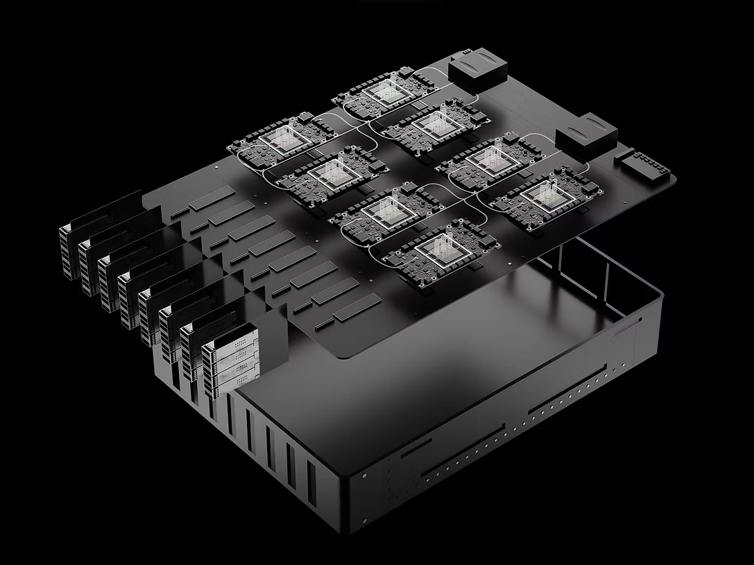
Neurophos, an Austin-based semiconductor startup developing photonic AI accelerators, announced on January 22, 2026, that it has raised $110 million in a Series A funding round led by Gates Frontier, Bill Gates’ venture capital firm. The oversubscribed round brings the company’s total funding to $118 million and positions Neurophos as a potential disruptor in the AI chip market currently dominated by Nvidia’s graphics processing units.
The funding round attracted significant strategic participation beyond Gates Frontier. Microsoft’s venture fund M12, Carbon Direct Capital, Aramco Ventures, Bosch Ventures, Tectonic Ventures, and Space Capital all joined the round, alongside additional investors including DNX Ventures, Geometry, Alumni Ventures, MetaVC Partners, Silicon Catalyst Ventures, and others. This diverse investor base—spanning technology giants, energy companies, automotive manufacturers, and climate-focused funds—reflects the broad industrial implications of more efficient AI computing.
At the heart of Neurophos’s technology is a fundamentally different approach to AI computation. Rather than using electricity to move data through silicon transistors—the approach employed by every major AI chip on the market today—Neurophos’s optical processing unit (OPU) uses photons of light to perform calculations. This physics-level shift promises dramatic improvements in both speed and energy efficiency, potentially addressing two of the most pressing constraints facing the AI industry: power consumption and computational capacity.
The company’s proprietary innovation centers on what it calls micron-scale metamaterial optical modulators—specialized structures that manipulate light at extremely small scales to perform mathematical operations. Neurophos claims these modulators are approximately 10,000 times smaller than traditional optical computing components, enabling the integration of over one million optical processing elements on a single chip. This miniaturization breakthrough makes photonic computing practical for mass production using standard semiconductor manufacturing processes.
Dr. Patrick Bowen, Neurophos CEO and co-founder, emphasized the urgency driving the company’s development efforts. “Moore’s Law is slowing, but AI can’t afford to wait,” Bowen stated in the funding announcement. “Our breakthrough in photonics unlocks an entirely new dimension of scaling by packing massive optical parallelism on a single chip. This physics-level shift means both efficiency and raw speed improve as we scale up, breaking free from the power walls that constrain traditional GPUs.”
The performance claims are striking. Neurophos asserts its chips can deliver up to 100 times the performance and energy efficiency of current leading AI accelerators while functioning as a drop-in replacement for existing GPUs in data centers. In early testing, the company has demonstrated performance exceeding 300 trillion operations per second per watt—far surpassing existing silicon-based standards. If these metrics hold in production environments, photonic chips could fundamentally reshape the economics of AI inference and training.
The company’s technology emerged from research conducted at Duke University, where co-founders Bowen and Dr. Andrew Traverso worked on metamaterials—engineered structures with optical properties not found in nature. This research initially explored exotic applications like optical cloaking and invisibility, but the team recognized that the same principles could enable revolutionary advances in computing. Neurophos spun out from Metacept, an incubator run by David Smith, a prominent metamaterials researcher.
Microsoft’s engagement with Neurophos extends beyond financial investment. Dr. Marc Tremblay, Corporate Vice President and Technical Fellow of Core AI Infrastructure at Microsoft, provided a statement emphasizing the strategic importance of the technology: “Modern AI inference demands monumental amounts of power and compute. We need a breakthrough in compute on par with the leaps we’ve seen in AI models themselves, which is what Neurophos’ technology and high-talent density team is developing.”
The timing of Neurophos’s emergence reflects growing concerns about the sustainability of current AI scaling trajectories. Large language models and other AI systems have grown exponentially more computationally expensive, with training costs for frontier models now measured in hundreds of millions of dollars. Simultaneously, the energy consumption of AI data centers has become a political and environmental issue, with some localities blocking new facility construction due to power grid constraints.
Photonic computing offers theoretical advantages that could address these challenges. Light travels faster than electrons, produces less heat, and is less susceptible to electromagnetic interference. Optical components can carry multiple wavelengths simultaneously, enabling massive parallelism. However, photonic computing has historically struggled with practical challenges: optical components tend to be larger than their silicon counterparts, conversion between digital and analog signals consumes power, and manufacturing at scale has proven difficult.
Neurophos believes its metasurface modulators solve these problems. The extreme miniaturization enables chip-scale integration, while the design reportedly works with standard silicon foundry processes, materials, and tools—critical factors for economically viable mass production. The company has not disclosed which foundry partners it plans to use, though successful commercialization will likely require collaboration with advanced semiconductor manufacturers like TSMC or Intel.
The fresh capital will accelerate Neurophos toward its first product milestone: delivery of integrated photonic compute systems by early 2028. This timeline includes developing datacenter-ready OPU modules, creating a complete software stack to interface with existing AI frameworks, and providing early-access developer hardware. The company is also expanding its Austin headquarters and opening a new engineering office in San Francisco to attract talent and engage with potential customers in the Bay Area’s tech ecosystem.
Michael Stewart, Managing Partner at M12, indicated that institutional investors view the development timeline as credible. “The team has progressed from proof of concept to a product timeline that institutions are willing to underwrite,” Stewart noted. This assessment suggests Neurophos has moved beyond pure research into engineering development, a critical transition for deep-tech startups seeking commercial viability.
The competitive landscape for alternative AI accelerators is intensifying. While Nvidia maintains overwhelming market dominance—with a market capitalization exceeding $3 trillion driven primarily by AI chip sales—multiple startups and established companies are pursuing different approaches. Cerebras Systems builds wafer-scale chips, Groq focuses on software-defined hardware, and other photonics companies like Lightmatter have pivoted to focus on optical interconnects rather than compute. AMD and Intel continue developing silicon-based alternatives to Nvidia’s offerings.
What distinguishes Neurophos’s approach is the radical departure from silicon-based computation entirely. Rather than incremental improvements to existing architectures, photonic processing represents a fundamentally different computing paradigm. Success would validate the physics principles underlying the technology and potentially open pathways to even more advanced optical computing systems. Failure would raise questions about whether theoretical advantages can translate to practical, economically viable products.
The Norwegian data center operator Terakraft has already signed on to pilot Neurophos technology, with a real-world deployment planned for 2027. This early customer engagement suggests some data center operators are willing to test alternative architectures despite the risks inherent in unproven technology. Success in this pilot could catalyze additional adoption, while challenges could slow the path to commercialization.
Industry observers note that even if Neurophos succeeds technically, market adoption will require overcoming Nvidia’s ecosystem advantages. Software developers have optimized AI frameworks around CUDA, Nvidia’s programming interface, creating significant switching costs. Data center operators have invested in Nvidia-specific infrastructure, power systems, and operational processes. Displacing an incumbent with these advantages demands not just superior performance but substantially superior performance that justifies transition costs.
Nevertheless, the strategic investors backing Neurophos appear convinced the potential rewards justify the risks. Climate-focused investors like Carbon Direct see photonic computing as essential for reducing AI’s carbon footprint. Energy companies like Aramco Ventures recognize that more efficient computing could reduce infrastructure demands. Technology leaders like Microsoft understand that breaking free from silicon’s limitations may be necessary for continued AI advancement.
For the AI industry broadly, Neurophos’s progress—regardless of ultimate commercial success—signals growing recognition that silicon-based approaches may have fundamental limits. As AI models continue growing in size and complexity, the industry may need multiple complementary technologies: silicon for some workloads, photonics for others, and potentially entirely new approaches still in research labs. The next few years will determine whether light-based computing moves from scientific curiosity to commercial reality.


