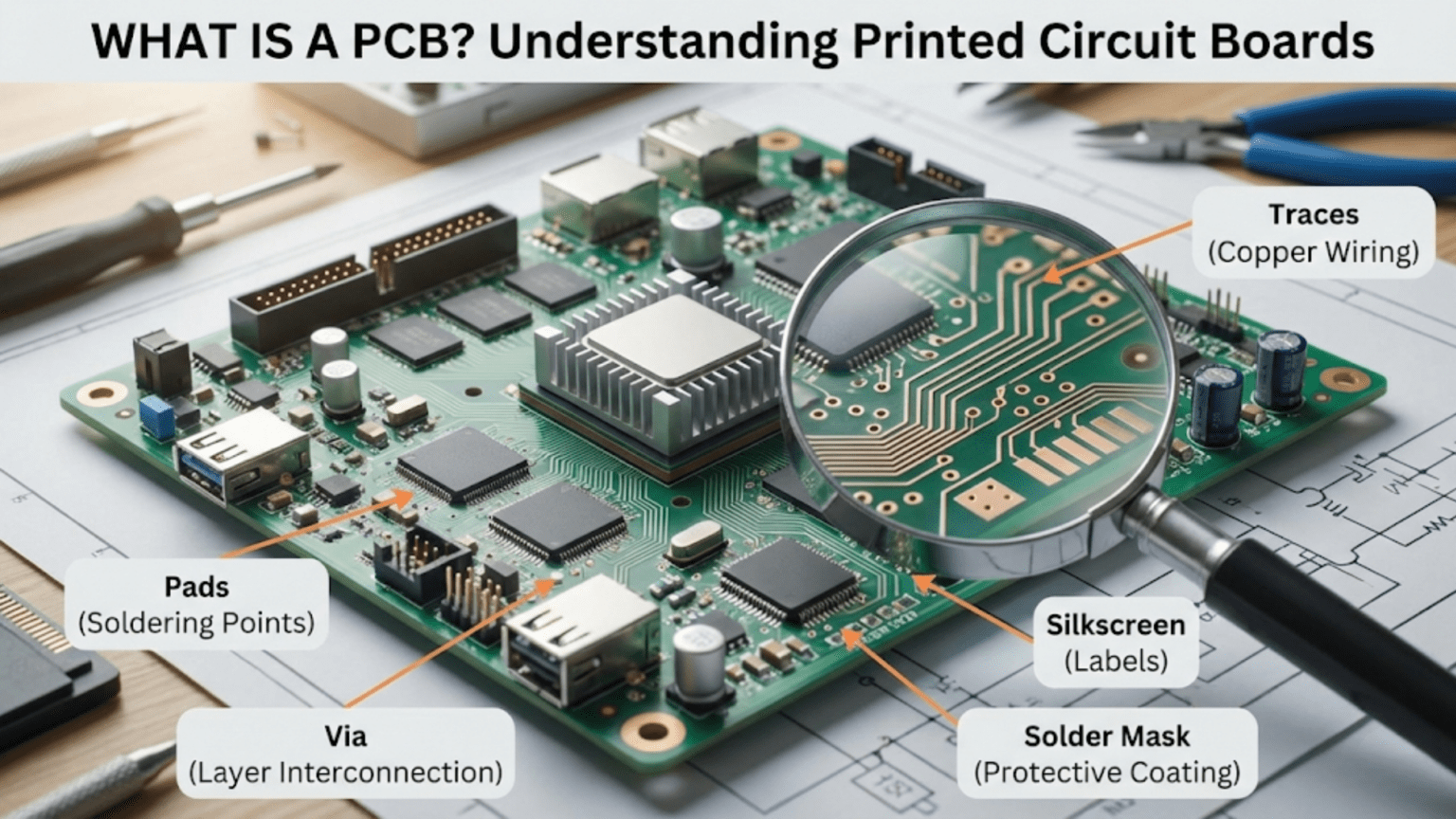
A PCB (Printed Circuit Board) is a flat board made of insulating material, most commonly FR4 fiberglass, with thin layers of copper etched into precise patterns called traces that electrically connect components soldered to its surface. PCBs replaced the tangle of hand-wired point-to-point connections that characterized early electronics, providing a compact, repeatable, and manufacturable platform where resistors, capacitors, ICs, and other components mount in fixed positions and interconnect through the copper trace network to form complete functional circuits.
Introduction: The Foundation of Modern Electronics
Pick up any electronic device—a smartphone, a TV remote, a smoke detector, a car’s engine control unit—and inside you’ll find one or more printed circuit boards. PCBs are so ubiquitous that the modern electronics industry would simply not exist without them. Yet despite being the literal foundation on which every electronic circuit stands, many beginners treat PCBs as a given, understanding them superficially as “the green board with stuff soldered on it” without appreciating the remarkable engineering that goes into their design and manufacture.
Understanding PCBs deeply changes how you think about electronics. You stop seeing circuits as abstract collections of schematic symbols and start seeing them as physical objects with spatial relationships, current paths, and thermal challenges. You begin to understand why some circuits work on a breadboard but fail when transferred to a PCB (layout problems, ground impedance, coupling). You develop insight into why high-speed digital circuits require careful trace routing, why power supply decoupling must be placed close to ICs, and why a ground plane dramatically improves noise performance.
The story of PCBs is also the story of how electronics became affordable, reliable, and miniaturized enough to permeate every aspect of modern life. Before PCBs, electronics meant chassis full of vacuum tubes, hand-wired between terminal posts, with technicians spending days assembling and testing individual units. Each unit was unique, handmade, and expensive. PCBs enabled automation: a single PCB design could be replicated millions of times with consistent quality, transforming electronics from a luxury into a commodity.
This comprehensive guide explores printed circuit boards from first principles through practical application. We’ll examine what a PCB actually is at a material and physical level, trace the history of how PCBs came to dominate electronics, understand the layers that make up a modern PCB, explore the manufacturing process, survey different PCB types and their applications, and develop the foundational understanding that enables you to read, modify, and eventually design your own boards.
Whether you’re a beginner who just received their first Arduino and wonders what the green board actually is, or an intermediate hobbyist ready to design your first custom PCB, this guide builds the understanding you need.
What a PCB Is: The Physical Reality
The Core Components of a PCB
A printed circuit board is a precisely engineered sandwich of materials, each serving a specific function:
1. Substrate (Core Material) The structural foundation of the PCB—the insulating base onto which copper layers are laminated. The substrate must be:
- Electrically non-conductive (isolates copper layers from each other and the environment)
- Dimensionally stable (doesn’t warp or expand significantly with temperature)
- Mechanically strong (supports components and survives handling)
- Heat resistant (withstands soldering temperatures)
- Chemically inert (resists flux, solvents, and moisture)
FR4 — the universal standard: The vast majority of PCBs use FR4 (Flame Retardant 4), a composite material consisting of woven fiberglass cloth impregnated with an epoxy resin. The name refers to the UL94 V-0 flame retardant specification it meets.
FR4 properties:
- Dielectric constant: ~4.5 (affects high-frequency signal behavior)
- Glass transition temperature (Tg): 130–180°C depending on grade
- Moisture absorption: Low (<0.10% by weight)
- Color: Typically yellow-green, though visible only at board edges (copper and soldermask cover the surface)
- Thickness: Standard 1.6mm, though 0.8mm, 1.0mm, 2.4mm also common
Other substrate materials:
- CEM-1, CEM-3: Composite epoxy material, cheaper than FR4, used in low-cost consumer electronics
- Polyimide (Kapton): Used in flexible PCBs; excellent thermal stability
- PTFE (Teflon): Used in RF/microwave circuits; very low dielectric constant
- Aluminum-core: Used in LED lighting; excellent thermal conductivity
- Rogers: High-frequency laminate for microwave applications
2. Copper Layers Thin copper foil, electrodeposited or rolled, laminated to the substrate surfaces. Copper is used because it combines excellent electrical conductivity, good solderability, the ability to be chemically etched into fine patterns, and reasonable cost.
Copper weight: Measured in ounces per square foot of coverage:
- 1 oz copper: Approximately 35 micrometers (35μm) thick — standard for most signal layers
- 2 oz copper: ~70μm — used for power layers requiring higher current capacity
- 0.5 oz copper: ~17.5μm — used for very fine trace work
What copper forms:
- Traces: Narrow pathways that carry current from point to point (the “wires” of the PCB)
- Pads: Larger copper areas where component leads are soldered
- Vias: Holes with plated copper walls connecting copper on different layers
- Planes: Large solid copper areas covering most of a layer (ground planes, power planes)
- Polygons/pours: Filled copper areas covering irregular shapes
3. Soldermask The colored coating that covers most of the board’s copper surface. This is typically what gives PCBs their characteristic green color (though blue, red, black, white, yellow, and other colors are available).
Soldermask functions:
- Protects copper traces from oxidation and environmental damage
- Prevents solder from flowing onto traces during soldering (keeping solder on pads only)
- Provides electrical insulation between closely spaced traces
- Reduces the risk of solder bridges on fine-pitch pads
- Provides a contrasting background for silkscreen printing
Soldermask opening: Everywhere a pad needs to be soldered, the soldermask is removed (“opened”), exposing the copper pad beneath. These openings precisely define the solderable areas.
4. Silkscreen (Legend) The printed text and symbols on the PCB surface — reference designators (R1, C3, U2), polarity marks, component outlines, board revision numbers, manufacturer logos, and any other human-readable information.
Silkscreen is printed over the soldermask using screen printing or inkjet printing. It’s purely informational—it has no electrical function—but it’s invaluable during assembly, debugging, and repair.
5. Surface Finish The soldermask openings expose bare copper pads, but bare copper oxidizes rapidly and solders inconsistently. Surface finish is a thin coating applied to exposed pads to protect them and ensure good solderability.
Common surface finishes:
- HASL (Hot Air Solder Leveling): Pads dipped in liquid solder, excess blown off with hot air. Inexpensive, robust, good solderability. Creates slightly uneven surface (less ideal for fine-pitch SMD)
- Lead-free HASL: Same process with lead-free solder
- ENIG (Electroless Nickel Immersion Gold): Thin gold layer over nickel. Flat surface (excellent for SMD), good shelf life, compatible with aluminum wire bonding. More expensive; gold dissolves into solder during reflow
- ENEPIG: Electroless nickel, electroless palladium, immersion gold — highest reliability, used in semiconductor packages
- Immersion Silver: Flat, good for fine-pitch, somewhat sensitive to handling and storage (tarnishes)
- OSP (Organic Solderability Preservative): Thin organic coating on copper. Least expensive, flat surface, limited shelf life
PCB History: From Wire Chaos to Silicon Substrate
Before PCBs: Point-to-Point Wiring
Early electronic devices—radios, amplifiers, early computers—used a technique called point-to-point wiring. Components (resistors, capacitors, vacuum tubes) were mounted on a chassis, and connections between them were made with individual wires, each hand-soldered between terminal points.
Point-to-point wiring was:
- Labor-intensive: Each unit required hours of skilled hand assembly
- Variable: Each unit was unique; quality depended on individual assemblers
- Difficult to repair: Finding a specific connection in a tangle of wires was challenging
- Bulky: Wires needed physical separation to avoid shorts
- Not mass-producible: No automated path forward
A skilled technician could build quality point-to-point circuits, but scaling production was nearly impossible. As electronic devices became more complex and demand grew, a better approach was urgently needed.
The Invention of the PCB
Paul Eisler (1936): Austrian engineer Paul Eisler is widely credited with inventing the printed circuit board in the mid-1930s while working in England. He developed the technique of printing a conducting material onto an insulating base to create an electric circuit—hence “printed” circuit board.
Eisler patented his process in 1943, and the technology was used in proximity fuses during World War II—perhaps the first high-volume electronic product to use printed circuits.
Post-war adoption: After WWII, the US Army and Navy released the technology, and it slowly spread to commercial electronics. The first consumer radio using a PCB appeared in the early 1950s.
The transistor revolution accelerates PCB adoption: When transistors replaced vacuum tubes (starting in the mid-1950s), they were smaller, operated at lower voltages, and generated less heat. PCBs were perfectly suited to the transistor era in ways they hadn’t been for bulky vacuum tubes. Through the 1960s, PCBs became standard.
The integrated circuit era: The invention of the integrated circuit (1958–1959) placed multiple transistors on a single chip. ICs enabled enormous complexity in small packages—but only if those ICs could be interconnected efficiently. PCBs became essential infrastructure for IC-based systems.
PCB Technology Evolution
Single-layer PCBs (1950s–1960s): Copper traces on one side only. Components mounted on one side, soldered on the other. Simple and inexpensive but limited in routing density.
Double-layer PCBs (1960s onwards): Copper on both sides, connected by drilled and plated holes (vias). Dramatically increased routing density.
Multi-layer PCBs (1970s onwards): Multiple copper layers sandwiched inside the substrate, connected by vias. Enabled dense, complex routing for computers and professional electronics.
Surface mount technology (1980s): Components mounted directly on the surface of the PCB rather than through holes. Enabled smaller components, double-sided mounting, and automated pick-and-place assembly. Transformed PCB manufacturing productivity.
HDI (High-Density Interconnect, 1990s–present): Very fine traces, micro-vias (laser-drilled), and multiple build-up layers enable the extremely dense PCBs found in smartphones and tablets.
PCB Layers: Understanding the Stack-Up
Single-Layer PCBs
The simplest form: one copper layer on one side of the substrate.
Structure:
- Top: Substrate (bare)
- Middle: FR4 substrate
- Bottom: Copper traces + soldermask + silkscreen
Use cases: Very simple circuits, low-cost consumer products, some LED boards, simple power supplies.
Limitations: All routing must fit on one side; crossovers require jumper wires.
Double-Layer (Two-Layer) PCBs
Two copper layers, one on each side of the substrate, connected by through-hole vias.
Structure:
- Top: Copper (traces, pads) + soldermask + silkscreen
- Core: FR4 substrate
- Bottom: Copper (traces, pads) + soldermask + optional bottom silkscreen
Use cases: Most hobby electronics, Arduino shields, moderate-complexity designs, small single-board computers. The most common PCB type for hobbyist and small production work.
Vias in 2-layer boards: A via is a drilled hole, plated with copper on its interior walls, that electrically connects the top and bottom copper layers. A trace on top can connect to a trace on the bottom by routing through a via.
Via types:
- Through-hole via: Drills all the way through the board. Standard for 2-layer boards.
- Blind via: Connects an outer layer to an inner layer without going all the way through
- Buried via: Connects two inner layers without reaching either outer surface
- Micro-via: Very small via (typically <0.15mm diameter), usually laser-drilled, used in HDI boards
Four-Layer PCBs
Four copper layers stacked with prepreg (pre-impregnated fiberglass bonding material) between them.
Typical layer assignment:
- Layer 1 (Top): Signal routing, component pads
- Layer 2: Ground plane (solid copper)
- Layer 3: Power plane (solid copper or split for multiple voltages)
- Layer 4 (Bottom): Signal routing
Why dedicated ground and power planes?
- Ground plane provides a low-impedance current return path for all signals
- Dramatically reduces ground noise and improves signal integrity
- Acts as electromagnetic shield between signal layers
- Power plane provides low-impedance distribution of supply voltage
- Reduces PCB complexity (traces don’t need to route power around)
Use cases: Microcontrollers, FPGAs, mixed analog-digital circuits, anything with moderate to high speed signals or where noise matters.
Six, Eight, and More Layer PCBs
Professional and high-complexity designs use six to sixteen or more layers. Each additional layer pair adds routing space and allows more dedicated planes.
A typical 6-layer stack:
- Layer 1: Signal (top)
- Layer 2: Ground plane
- Layer 3: Signal (high-speed)
- Layer 4: Power plane
- Layer 5: Ground plane
- Layer 6: Signal (bottom)
Applications: High-speed digital circuits, complex FPGAs, CPU boards, RF modules, smartphones.
Cost implications: Roughly, each layer pair doubles manufacturing cost. A 4-layer board costs approximately 3–4× a comparable 2-layer board; an 8-layer board perhaps 8–10×.
How PCBs Are Manufactured
From Design File to Finished Board
Step 1: PCB Design (EDA Software) The circuit starts as a schematic (logical connections) which is converted to a layout (physical arrangement of components and routing of traces). This is done in Electronic Design Automation (EDA) software such as KiCad (free, open-source), Altium Designer (professional), Eagle, or many others.
The layout produces Gerber files—industry-standard format describing each layer of the PCB as 2D vector graphics.
Step 2: Design Rule Check (DRC) Before manufacture, the design is checked against manufacturing constraints (minimum trace width, minimum via size, minimum pad-to-pad spacing). Violations are flagged and corrected.
Step 3: Manufacturing the Core FR4 cores start as large panels (typically 18″×24″ or similar). The copper-clad laminate is inspected, then processed.
Step 4: Photolithography — Patterning the Copper The copper surface is coated with photoresist (light-sensitive material). The Gerber files are used to create a photomask (a film or glass plate with the trace patterns). UV light exposes the photoresist through the mask. Chemical developer removes unexposed resist. Etchant (typically ferric chloride or ammonium persulfate) dissolves unprotected copper, leaving only the traces and pads defined by the design. Remaining resist is stripped.
Step 5: Layer Lamination (Multi-Layer Boards) For multi-layer boards, individual etched layers are stacked with prepreg (partially cured fiberglass-resin sheets) between them. The stack is pressed in a hydraulic press at high temperature and pressure, fusing everything into a solid panel.
Step 6: Drilling CNC drill machines drill all required holes: component through-holes, via holes, mounting holes. Drill bits are precisely positioned to within ±0.05mm or better.
For micro-vias (HDI boards), laser drilling achieves holes as small as 0.1mm.
Step 7: Through-Hole Plating Drilled holes are electrolessly plated with copper, then electrolytically plated to the required thickness. This creates the conductive barrel inside each via, connecting layers.
Step 8: Outer Layer Processing Top and bottom copper layers are patterned using the same photolithography process as inner layers.
Step 9: Soldermask Application Liquid photo-imageable soldermask is applied (typically sprayed or curtain-coated), exposed through a mask, and developed to open the pad areas. Then thermally cured.
Step 10: Silkscreen Printing Reference designators, polarity marks, and other markings printed onto the soldermask surface.
Step 11: Surface Finish HASL, ENIG, or other surface finish applied to exposed copper pads.
Step 12: Electrical Testing Automated test equipment (ATE) probes every net on the board, verifying continuity and isolation. Detects manufacturing defects like opens and shorts.
Step 13: Routing and V-Scoring Individual boards are separated from the manufacturing panel by routing (milling) or V-scoring (scoring V-shaped grooves for breaking apart).
Step 14: Final Inspection and Packaging Visual inspection (automated optical inspection, AOI, and sometimes manual), then boards are packaged for shipment.
Prototype vs. Production Manufacturing
Prototype PCB services (e.g., JLCPCB, PCBWay, OSHPark, Oshpark):
- Minimum quantities as low as 5 boards
- Turnaround: 24–72 hours for standard specs
- Cost: $2–10 for 5 simple 2-layer boards (remarkable value!)
- Limited stackup options, standard specs only
- Widely used by hobbyists and small companies
Production PCB manufacturing:
- Quantities from hundreds to millions
- Optimized for specific tolerances and specifications
- Volume pricing reduces per-board cost dramatically
- Full specification flexibility
- Longer lead times for custom specifications
Types of PCBs
Rigid PCBs
The standard PCB type — inflexible boards made of FR4 or similar rigid laminate. Components are permanently mounted in fixed positions.
Applications: Literally everything — computers, phones, appliances, instruments, vehicles.
Flexible PCBs (Flex PCBs)
Made from flexible polyimide (Kapton) substrate with thin copper traces. Can be bent, folded, or formed into three-dimensional shapes.
Applications:
- Ribbon cables between PCB sections in laptops, phones
- Wearable electronics
- Camera modules (connects to main board with flex cable)
- Medical implants
- Any application requiring a dynamic flex or compact folded routing
Rigid-Flex PCBs: Combined rigid and flexible sections in a single board. Rigid sections carry components; flex sections connect them. Used in compact consumer electronics (phones, laptops).
Metal-Core PCBs (MCPCBs)
Aluminum or copper core substrate provides dramatically better thermal conductivity than FR4. Heat generated by components spreads through the metal core and dissipates efficiently.
Applications:
- High-power LED lighting
- Motor drive circuits
- Power amplifiers
- Any application where component thermal management is critical
High-Frequency PCBs
Specialized substrates (Rogers, PTFE, Isola) with controlled dielectric properties for RF and microwave applications.
Why standard FR4 fails at high frequencies: FR4’s dielectric constant (~4.5) varies with frequency and temperature, causing signal velocity variation, insertion loss, and crosstalk that degrade RF performance above about 1–2 GHz.
Applications: Antenna boards, radar systems, satellite communications, 5G infrastructure.
Embedded Component PCBs
Components (especially capacitors and resistors) embedded within the PCB layers rather than mounted on the surface. Ultra-compact, excellent electrical performance, expensive.
Applications: High-density modules, certain smartphone components.
Reading a PCB: What You’re Looking At
The Top-Side View
Looking at the component side of a typical PCB, you see:
The soldermask: Green (or another color), covering most of the surface. This is the PCB’s “skin.”
Exposed copper pads: Shiny metallic areas (silver-colored if ENIG/immersion silver, or slightly gray if OSP). These are where components are soldered.
Silkscreen markings:
- Reference designators: R1, C4, U2, J1 — identify each component’s position
- Polarity indicators: + symbols, stripes, pin 1 dots, triangle markers
- Component outlines: White rectangles or shapes showing where component bodies sit
- Board information: Revision number, board name, manufacturer, date code
Component packages (typical):
- DIP ICs: Dual inline package, two rows of pins
- SOIC, TSSOP: Surface-mount IC packages
- 0402, 0603, 0805: Surface-mount resistors/capacitors (size codes in inches × 100)
- TO-220, TO-92: Through-hole transistor packages
- Headers/connectors: Row of pins or sockets
The Bottom-Side View
For through-hole boards: Lead stubs and solder fillets are visible on the bottom — the actual solder joints.
For SMD boards: More components (sometimes all components are double-sided), and through-hole via solder points.
Bottom silkscreen: Often present, usually less dense than top. May show board outline, test points, or additional markings.
Reading Traces
Traces are the copper pathways between pads. On a simple 2-layer board with no soldermask (bare copper), you can see traces directly. On a finished board with soldermask, traces are hidden under the soldermask but their paths can often be inferred.
Trace width significance:
- Narrow traces: Signal lines carrying milliamps
- Wide traces: Power distribution carrying amps
- Very wide copper pours: Ground connections, power planes
- A trace running to multiple component pads: Bus or shared signal
PCB Design Software: Creating Your Own
The PCB Design Process
Creating a PCB involves two main steps:
1. Schematic capture: Drawing the logical circuit — which components connect to which, using standard schematic symbols. The schematic defines the netlist (what’s connected to what) but not physical layout.
2. PCB layout: Placing components on the board outline and routing copper traces between their pads according to the netlist. This is where spatial decisions are made: where does each component go? How do traces route between them? How wide are power traces? Where are decoupling capacitors placed?
Popular PCB Design Software
KiCad (free, open-source): The most popular free PCB design tool. Full-featured schematic and layout capabilities. Active community, extensive component libraries, widely supported by PCB manufacturers. Recommended for hobbyists and small companies.
EasyEDA (free, web-based): Browser-based tool with deep integration with JLCPCB (the most popular budget PCB manufacturer) and LCSC (component supplier). Very low barrier to entry. Good for simpler designs.
Altium Designer (professional, expensive): Industry-leading professional tool. Extremely capable for complex designs. Used in most professional electronics companies. Student licenses available.
Eagle (now Fusion 360 Electronics): Once dominant in hobbyist community, now owned by Autodesk. Still widely used, large library. Freemium model.
Fusion 360 Electronics: Autodesk’s updated version of Eagle. Integrated with mechanical design tools.
From Design to Manufactured Board
Modern PCB manufacturing services accept Gerber files (industry standard) or in some cases native KiCad/EasyEDA files directly.
The typical flow:
- Draw schematic in EDA software
- Create PCB layout (place components, route traces)
- Run DRC (design rule check) to catch errors
- Export Gerber files
- Upload to PCB service (JLCPCB, PCBWay, OSHPark, etc.)
- Review online preview (most services show rendered boards)
- Place order (minimum quantities typically 5)
- Wait 1–3 weeks for delivery (or 3–5 days with express)
- Solder components and test
Comparison Table: PCB Types and Characteristics
| PCB Type | Layers | Substrate | Flexibility | Cost (relative) | Typical Applications | Key Advantage |
|---|---|---|---|---|---|---|
| Single-layer rigid | 1 | FR4 | None | Very low | Simple circuits, lighting | Cheapest, simplest |
| Double-layer rigid | 2 | FR4 | None | Low | Hobby, moderate complexity | Best value for most projects |
| 4-layer rigid | 4 | FR4 | None | Moderate | Microcontrollers, mixed signal | Ground/power planes |
| 6+ layer rigid | 6–20 | FR4/specialty | None | High | Complex digital, RF | Maximum routing density |
| Flexible | 1–2 | Polyimide | High | Moderate–high | Wearables, ribbon cables | Bends and folds |
| Rigid-flex | Mixed | FR4 + Polyimide | Partial | High | Phones, cameras | Best of both worlds |
| Metal-core | 1–2 | Aluminum/copper | None | Moderate | LED lighting, power circuits | Thermal management |
| High-frequency | 2–8 | Rogers/PTFE | None | Very high | RF, radar, 5G | Controlled impedance at GHz |
| HDI | 4–20 | FR4 specialty | None | Very high | Smartphones, dense modules | Ultra-fine pitch density |
Why PCB Design Decisions Matter
Component Placement Philosophy
Place before routing: Component placement determines routing options. Poor placement makes routing difficult or impossible. Good placement makes routing nearly automatic.
Decoupling capacitors: Must be placed as close as possible to the IC power pins they serve. Routing a long trace from the capacitor to the IC pin negates the capacitor’s function.
Signal flow: Place components so signals flow in a logical path — input to output, top-to-bottom or left-to-right. Reduces trace length and crossing.
Thermal considerations: High-power components need thermal management — either copper pours to spread heat, thermal vias to conduct heat to a metal-core board or heatsink, or physical separation from heat-sensitive components.
Trace Width and Current Capacity
Traces carry current and have resistance. Insufficient trace width causes:
- Voltage drop along the trace (especially problematic for power)
- Heat generation (I²R loss)
- Potential trace fuse (melting at very high current)
Approximate current capacity (1 oz copper, 10°C temperature rise):
- 0.25mm (10 mil): ~0.5A
- 0.5mm (20 mil): ~1.0A
- 1.0mm (40 mil): ~1.8A
- 2.0mm (80 mil): ~3.0A
Online calculators (based on IPC-2221 standard) give precise values for any trace width and copper weight.
Ground Planes and Signal Integrity
Perhaps the single most impactful PCB design decision for circuit performance is whether to use a ground plane.
Without ground plane: Current returns through whatever ground traces are routed. Each trace has resistance and inductance. Multiple circuits sharing ground traces create common impedance coupling (noise between circuits).
With ground plane: Every signal has a direct, low-impedance return path immediately beneath it. Noise coupling between circuits is minimized. The plane acts as an electromagnetic shield between layers.
For any circuit beyond simple power supplies, a dedicated ground plane layer (available on 4-layer boards, formed as a copper pour on 2-layer boards) dramatically improves performance.
Conclusion: The PCB as an Engineering Achievement
The printed circuit board represents one of the most consequential engineering achievements of the 20th century. It transformed electronics from a craft into a manufacturable technology, enabling the miniaturization and cost reduction that brought computing, communication, and intelligent devices to billions of people.
What You Now Understand
The PCB’s physical structure: FR4 substrate, copper layers, soldermask, silkscreen, surface finish — each layer serving a specific physical purpose.
How copper carries current: Traces route electrical connections, pads accept component solder joints, planes distribute power and return signal currents, vias connect layers.
PCB types: Single and double layer for simple work, four and more layers for professional complexity, flexible for bendable applications, metal-core for thermal management.
Manufacturing: From Gerber files through photolithography, drilling, plating, and finishing — a sophisticated process now accessible to hobbyists through inexpensive prototype services.
Design impact: Placement affects routing; trace width affects current and voltage drop; ground planes transform noise performance; all physical decisions have electrical consequences.
The Journey Forward
Understanding what a PCB is leads naturally to learning how to design one. The skills build progressively:
- Reading existing schematics and PCBs — understanding how others solved design problems
- Modifying and adapting designs — changing values, adding features to existing layouts
- Designing from scratch — schematic capture, component selection, layout, DRC, Gerber export
- Advanced topics — impedance-controlled traces, EMC design, thermal simulation, design for manufacture
The path from “what is a PCB?” to “I designed and built this PCB from scratch” is entirely accessible to self-taught hobbyists. Free tools (KiCad), inexpensive manufacturing ($2–5 for 5 boards), and a wealth of online resources make PCB design one of the most achievable advanced electronics skills.
A Final Perspective
Every time you use a modern electronic device, you’re benefiting from thousands of PCB design decisions: trace widths chosen to carry just enough current, decoupling capacitors placed to suppress just the right frequency noise, layer counts selected to fit required signal count within a physical envelope, ground planes preventing interference between circuits. Invisible, unglamorous, and essential — PCBs are genuinely the foundation on which modern electronics is built.
Understanding them, even at a conceptual level, fundamentally enriches your electronics practice. You see circuits not just as logical abstractions but as physical realities where space, material, and geometry matter just as much as Ohm’s Law.
The PCB isn’t just the green board. It’s the substrate of the modern world.