A PCB schematic is a standardized diagram that shows the logical electrical connections between components using universal symbols—resistors as zigzag lines or rectangles, capacitors as parallel lines, ICs as rectangles with labeled pins—connected by lines called nets that represent electrical connections regardless of physical distance. Reading a schematic requires recognizing component symbols, understanding net connections (including named nets that connect across the diagram without drawn lines), identifying power and ground symbols, following signal flow from input to output, and then translating those logical connections into a physical PCB layout where components occupy real space and copper traces follow specific routing paths.
Introduction: The Language Electronics Engineers Share
A schematic is the universal language of electronics. Regardless of which country designed a circuit, which company manufactured the PCB, or which decade the design was created, a schematic communicates the same information in the same way to any electronics engineer worldwide. Learning to read schematics fluently is one of the highest-leverage skills in electronics—it unlocks the ability to understand any circuit, replicate any design, diagnose any fault, and eventually create your own original circuits.
Yet many beginners approach schematics with unnecessary anxiety. The symbols look cryptic at first glance, the lines crossing the page seem chaotic, and the connection between the abstract diagram and the physical board of components seems mysterious. In reality, schematics follow consistent conventions that, once learned, make circuits remarkably transparent. A schematic that initially looks like a meaningless tangle reveals itself—with knowledge—as a precisely organized logical map of how electricity flows through a circuit.
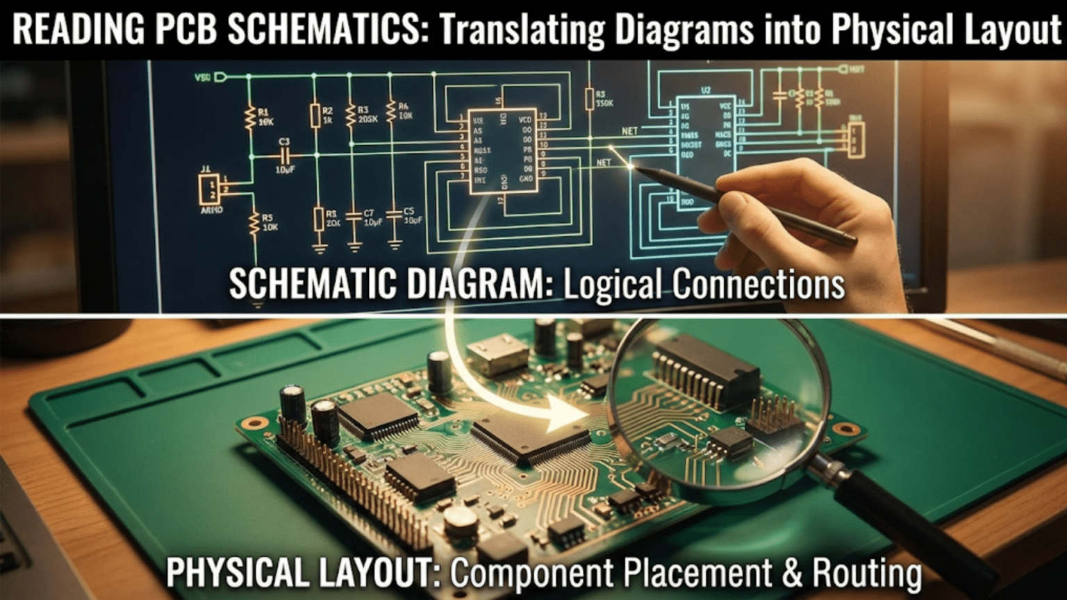
The step from schematic to physical layout adds another layer of complexity. A schematic shows what connects to what, but it deliberately ignores where things are physically located. Translating a schematic into a PCB layout requires understanding which components should sit near each other for electrical reasons (decoupling capacitors close to IC power pins), which should be separated (digital noise generators away from sensitive analog inputs), how traces route between pads without crossing in forbidden ways, and how the physical constraints of space, layers, and manufacturing tolerances shape every routing decision.
This guide develops schematic reading as a complete skill, from recognizing individual symbols through understanding complete circuits, then extends that knowledge into the physical world of PCB layout. We’ll build vocabulary systematically, work through real circuit examples, understand the conventions that make schematics unambiguous, and develop the mental bridge between abstract diagram and physical board that separates people who can truly read electronics documentation from those who are just guessing.
Whether you’ve never seen a schematic before, can recognize most symbols but struggle to follow complex diagrams, or want to develop the skill of translating schematics into PCB layouts, this guide builds the complete foundation.
The Purpose and Philosophy of Schematics
What a Schematic Shows (and What It Doesn’t)
A schematic communicates one thing above all else: which electrical nodes are connected to which other nodes through which components.
A schematic tells you:
- Which components are in the circuit (by type and value)
- How those components are electrically interconnected
- The logical flow of signals and power through the circuit
- Reference designators for identifying specific components
- Net names for identifying specific electrical nodes
A schematic deliberately does NOT tell you:
- Where components are physically located on the board
- How long traces are
- Which layer traces run on
- Component physical size or orientation on the PCB
- How close together components are mounted
This deliberate separation of logical (schematic) and physical (layout) information is intentional and powerful. It allows circuit designers to think about electrical function without being distracted by physical implementation, and it allows the same logical circuit to be implemented in many different physical forms—different PCB sizes, different component orientations, different trace routings—while remaining electrically identical.
The Net: The Fundamental Schematic Concept
The most important concept in schematic reading is the net (also called a node or signal).
A net is a set of component pins that are all electrically connected together. Any component pins connected by drawn lines in a schematic, or sharing the same net name, are part of the same net—they are at the same voltage at all times (ignoring parasitic effects).
Example: If a schematic shows: Battery positive terminal — wire — resistor left pin, and Battery positive terminal — wire — LED anode, then the battery positive terminal, the left pin of the resistor, and the LED anode are all on the same net. They will all be at the same voltage when the circuit operates.
Why nets matter: When reading a schematic, you’re essentially mapping out all the nets in the circuit. Once you know every net and which component pins connect to it, you understand the circuit completely from a logical standpoint.
Signal Flow Convention
Good schematics are drawn to guide the reader’s eye in the direction of signal flow:
Standard conventions:
- Left to right: Input signals enter from the left, output signals leave to the right
- Top to bottom: Power enters from the top, ground is at the bottom
- Higher voltages: Drawn higher on the page
- Lower voltages and ground: Drawn lower on the page
Not all schematics follow these conventions perfectly, especially complex designs with many interconnections, but understanding them helps you quickly orient yourself in an unfamiliar diagram.
Core Schematic Symbols
Resistors
US/ANSI symbol: Zigzag line (multiple peaks and valleys) IEC/European symbol: Rectangle with leads extending from each end
Both represent the same component. Modern electronics documentation increasingly uses the rectangular symbol even in US-produced designs.
Variations:
- Variable resistor (rheostat): Arrow through or alongside the zigzag/rectangle
- Potentiometer: Arrow between three terminals (two ends + wiper)
- Thermistor: NTC labeled with temperature symbol; PTC similarly
- Photoresistor (LDR): Resistor symbol with arrows pointing toward it (light input)
Schematic annotation:
- Reference designator: R1, R2, R3, etc.
- Value: 10kΩ, 470Ω, 2.2MΩ
- Power rating sometimes shown: 1/4W, 1W
- Tolerance shown for precision resistors: 1%, 0.1%
Capacitors
Non-polarized capacitor: Two parallel vertical lines (straight lines) Polarized capacitor (electrolytic/tantalum): One curved line (negative plate) and one straight line (positive plate), with + symbol on positive side
The curved line convention for polarized capacitors is critical—installing them backward causes violent failure. Always check the + marking on the schematic symbol.
Variations:
- Variable capacitor: Arrow through capacitor symbol
- Feed-through capacitor: Three-terminal symbol
- Trimmer/trimcap: Variable capacitor with adjustable arrow
Schematic annotation:
- Reference designator: C1, C2, C3
- Value: 100nF, 47μF, 10pF
- Voltage rating (important for polarized): 25V, 50V, 100V
- Tolerance for precision work: ±5%, ±20%
Inductors
Standard symbol: Series of humps or arcs (representing coil windings) Core variations:
- Air core: Plain arc series
- Iron core: Parallel lines beside the arcs
- Ferrite core: Dashed lines beside the arcs
- Toroidal: Curved core symbol
Variations:
- Transformer: Two coupled inductor symbols facing each other, often with vertical lines between representing the core
- Variable inductor: Arrow through inductor symbol
Schematic annotation:
- Reference designator: L1, L2
- Value: 10μH, 100mH, 1H
- Current rating for power inductors
Diodes
Standard diode: Triangle pointing in direction of conventional current flow, with a bar (vertical line) at the tip representing the cathode
Reading direction: Current flows in the direction the triangle points—from anode (flat side of triangle) to cathode (bar/line). The bar is the striped end of a physical diode.
Variations:
- Zener diode: Bar has bent ends (Z-shape)
- Schottky diode: Bar has curved ends
- LED (Light Emitting Diode): Diode symbol with arrows pointing away (light emission)
- Photodiode: Diode symbol with arrows pointing toward it (light input)
- Varactor diode: Diode symbol with capacitor-like bar
Transistors
BJT (Bipolar Junction Transistor):
- Three terminals: Base (B), Collector (C), Emitter (E)
- NPN: Arrow on emitter pointing away from base (Not Pointing iN)
- PNP: Arrow on emitter pointing toward base (Points iN Proudly)
The arrow mnemonic: “NPN — arrow Not Pointing iN (away from base). PNP — arrow Points iN.”
MOSFET (Metal-Oxide Semiconductor Field-Effect Transistor):
- Three terminals: Gate (G), Drain (D), Source (S)
- N-channel enhancement: Arrow pointing toward channel
- P-channel enhancement: Arrow pointing away from channel
- MOSFET body diode often shown explicitly
JFET: Different symbol, J-FET specific variants for N and P channel
Integrated Circuits (ICs)
Generic IC symbol: Rectangle with pins extending from one or more sides
Pin arrangements on IC schematic symbols:
- Pins are numbered and/or named
- Functions are often grouped logically (inputs on left, outputs on right)
- Power pins (VCC, GND) may be on top/bottom or grouped with other pins
- Pin 1 indicated by a dot, notch reference, or explicit numbering
Important: IC schematic symbols show logical pin groupings, NOT the physical pin positions on the chip package. Pin 1 on the schematic might be in the middle of one side of the physical chip; pin 14 might be directly above pin 7 on the schematic but across the chip physically.
Common IC types you’ll see:
- Op-amps: Triangle shape with +, − inputs and output, plus power pins
- Logic gates: AND, OR, NOT, NAND, NOR, XOR — each has a distinctive shape
- Voltage regulators: Often drawn as simple 3-pin rectangles
- Microcontrollers: Large rectangles with many named pins grouped by function
Power and Ground Symbols
These symbols represent connections to power and ground nets without drawing explicit wires to a power source. They’re one of the most important conventions for reading complex schematics.
Power symbols (VCC, VDD, +5V, +3.3V, etc.): Various conventions: small flag shape, upward-pointing lines, labeled arrows. Each distinct power net usually has its own symbol shape or label.
Ground symbols:
- Earth ground: Three horizontal lines, each shorter, like a downward triangle (actual earth ground, safety ground)
- Chassis ground: Circle with cross, or three diagonal lines
- Signal ground (0V reference): Downward-pointing triangle or three lines with flat bottom
- Digital ground (DGND), Analog ground (AGND): Labeled variations, important in mixed-signal designs
Critical convention: Every component connected to the same power symbol is connected to the same net. Multiple VCC symbols scattered across a schematic are all the same net. You don’t need a wire drawn between them—the identical symbol means the connection.
This is why: A complex schematic might show a capacitor connecting VCC to GND symbols with no visible connection to the IC it’s decoupling. The VCC symbol on the capacitor is the same net as the VCC pin on the IC, even though no line connects them. This keeps schematics readable by avoiding lines crossing the entire diagram.
Switches
SPST (Single Pole Single Throw): Single movable contact and single fixed contact — simplest switch SPDT (Single Pole Double Throw): One moving contact connects to one of two fixed contacts DPDT (Double Pole Double Throw): Two independent SPST switches mechanically linked Push button (momentary): NO (Normally Open) or NC (Normally Closed) variants
Connectors and Headers
Generic connector pin: Circle or square pad with pin number Male header: Pins represented as filled rectangles or circles in a row Female header: Open rectangles or circles Coaxial connector: Concentric symbols showing shield and center conductor
Connectors are identified by reference designator (J1, J2, CON1) and often include pin function labels.
Net Names and Power Flags: Implicit Connections
Named Nets
In any schematic more complex than a handful of components, drawing explicit wires between every connected pin creates an unreadable tangle. Named nets solve this problem.
How named nets work: A net name (label) attached to a wire identifies that wire as part of a named net. Any other wire in the schematic with the same label is connected to the same electrical node—no wire drawn between them.
Example: If the output pin of a voltage regulator has a label “VOUT” attached, and the power input pin of an IC several pages away also has a label “VOUT,” those two pins are connected—on the same net—even though no wire runs between them in the schematic.
Net name styles:
- Simple labels: VCC, GND, CLK, DATA
- Slash notation for active-low signals: /RESET, /CS (active when low)
- Overbar notation: signals with a bar over them are active-low
- Bus names: DATA[7:0] representing an 8-bit bus
Power Net Conventions
Common power net names and what they mean:
- VCC: Positive supply voltage for bipolar (BJT) circuits, historically collector supply
- VDD: Positive supply for FET/CMOS circuits, drain supply
- VEE: Negative supply (emitter supply for BJTs)
- VSS: Most negative supply or ground in CMOS circuits
- GND: Ground (0V reference)
- +5V, +3.3V, +1.8V: Explicit voltage references
- AVCC, AVDD: Analog supply voltage
- DVCC, DVDD: Digital supply voltage
- VBAT: Battery voltage (often separate from main supply)
Buses in Schematics
When many signals run in parallel (address bus, data bus, control signals), drawing individual lines for each would be impossibly cluttered. Buses solve this:
Bus representation: A thick line (or double line) represents multiple signals traveling together. Taps off the bus with individual net labels connect specific signals.
Example: An 8-bit data bus shows as one thick line labeled DATA[7:0]. Individual taps labeled D0 through D7 connect specific pins to specific bus lines.
Reading Reference Designators and Component Values
Reference Designator System
Every component in a schematic has a reference designator (refdes) — a letter code followed by a number.
Standard letter codes:
- R: Resistor (R1, R2, R47…)
- C: Capacitor (C1, C2, C100…)
- L: Inductor (L1, L2…)
- D: Diode (D1, D2…) — includes LEDs, Zeners
- Q: Transistor (Q1, Q2…) — BJTs and FETs
- U or IC: Integrated Circuit (U1, U2, IC1…)
- J or CON: Connector/Jack (J1, J2, CON1…)
- SW: Switch (SW1, SW2…)
- F: Fuse (F1, F2…)
- T: Transformer (T1, T2…)
- Y or XTAL: Crystal or oscillator (Y1, XTAL1…)
- TP: Test point (TP1, TP2…)
- FB: Ferrite bead (FB1…)
Numbers are assigned sequentially but don’t carry circuit meaning—R1 isn’t necessarily more important than R27.
Component Value Notation
Resistors:
- Ohms: 100Ω, 470Ω
- Kilohms: 4.7k, 10k, 100k (the Ω symbol often omitted)
- Megaohms: 1M, 2.2M
- European notation: 4k7 means 4.7kΩ; 4R7 means 4.7Ω (R = decimal point)
Capacitors:
- Picofarads: 100p, 22p (used for small ceramics)
- Nanofarads: 100n, 47n
- Microfarads: 0.1μF, 10μF, 100μF (electrolytics)
- Voltage rating always specified for polarized capacitors: 100μF/25V
Inductors:
- Nanohenries: 100nH, 47nH
- Microhenries: 10μH, 100μH
- Millihenries: 10mH, 100mH
Voltage regulators, transistors, ICs: Identified by part number (7805, LM317, 2N2222, ATmega328P) rather than value
A Step-by-Step Approach to Reading Any Schematic
Step 1: Identify Power Architecture
Before following any signal paths, understand how the circuit is powered:
- Find all power symbols (VCC, +5V, +3.3V, VBAT, etc.)
- Identify all ground symbols (GND, AGND, DGND)
- Locate the power supply or regulation circuit
- Note if multiple supply voltages exist (3.3V digital + 5V analog, for example)
- Understand which ICs run from which supply
Why first: Power connections affect everything. An IC drawn in the middle of the page connects to VCC and GND through those symbols—knowing the power architecture helps you understand every other part of the circuit.
Step 2: Identify Major Functional Blocks
Group the schematic into functional sections:
- Power supply and regulation
- Microcontroller or main IC
- Sensor inputs
- Output drivers (transistors, relays)
- Communication interfaces (UART, I2C, SPI)
- Connectors and user interface
Complex schematics often use visual grouping (dashed-line boxes), net labels that indicate function, or multiple schematic sheets each dedicated to one function.
Step 3: Follow Signal Flow
With functional blocks identified, trace signals from input to output:
- Start at the input (sensor, connector pin, user input)
- Follow the net from that input
- Note each component the signal passes through and how it’s modified
- Continue to the next stage
- End at the output (display, actuator, communication out)
Practical example — LED brightness control:
- Input: Potentiometer wiper (variable voltage)
- Net: BRIGHTNESS_ADJ
- To: Microcontroller ADC pin (reads voltage)
- Processing: MCU reads ADC value, generates PWM signal
- Net: LED_PWM
- To: Transistor base (through base resistor)
- Transistor switches LED cathode to ground
- LED connected between VCC and transistor collector
- Output: LED with brightness proportional to potentiometer position
Step 4: Identify Decoupling and Filtering Components
Schematic readers often skip the “boring” passive components near IC power pins. Don’t — they’re important:
- Every IC VCC pin should have at least one bypass capacitor (100nF ceramic typical) connecting to GND very nearby in the schematic
- Power supply outputs often have bulk capacitors (10–100μF electrolytic) plus ceramic bypass
- RC filters on sensitive inputs reduce noise
- Ferrite beads in power lines suppress high-frequency noise
Understanding why these components are there deepens schematic comprehension.
Step 5: Read Pin Functions, Not Just Connections
An IC pin labeled “ADC0” tells you far more than just “this is pin 23.” Understanding pin functions:
- Power pins (VCC, GND): Must be properly connected; missing power connections cause mysterious failures
- Reset pins: Active-low or active-high; external capacitor sometimes used for power-on reset
- Oscillator/crystal pins (XTAL1, XTAL2): Shows clock source
- Communication pins (TX, RX, SCL, SDA): Interface type and direction
- Interrupt pins (INT, IRQ): Shows what external events affect the MCU
- GPIO pins: General purpose, direction set in software
Reading pin function names on IC schematic symbols reveals the circuit’s operation even before you trace all the connections.
From Schematic to PCB Layout: The Translation
The Netlist: The Bridge Between Worlds
The transition from schematic to PCB layout happens through the netlist — a data file listing every net and which component pins belong to it.
In EDA software, the schematic capture tool exports a netlist that the PCB layout tool imports. This creates the electrical constraints the layout must satisfy: if the netlist says R1 pin 1 and U1 pin 3 are on net VCC, the PCB layout must connect those pads with copper (or they must both connect to a VCC power plane).
Ratsnest: When a netlist is imported into the PCB layout editor, “ratsnest” lines (thin, straight lines) appear connecting all the pads that belong to the same net. These lines show connections that need to be made with traces. As traces are routed, ratsnest lines disappear. The goal is to route all ratsnest connections and end with zero unrouted nets.
Translating Logic to Geometry: Key Principles
What the schematic doesn’t constrain (but the layout must decide):
Component placement: The schematic shows R1 connected to U1 pin 3, but doesn’t say whether R1 should be 1mm or 10mm from U1. Layout decides physical placement based on:
- Functional grouping (related components close together)
- Signal flow (components in the order signals pass through them)
- Electrical requirements (decoupling caps as close as possible to IC)
- Thermal requirements (heat generators away from sensitive components)
- Mechanical requirements (connectors at board edges, mounting holes in corners)
- Manufacturing requirements (adequate spacing between components)
Trace routing: The schematic shows a line connecting two pins, but the layout must find a physical path for that trace that:
- Doesn’t cross other traces on the same layer (or uses vias to change layers)
- Maintains adequate clearance to adjacent traces
- Meets width requirements for current capacity
- Avoids sensitive areas (near antennas, across split planes)
- Minimizes length for high-frequency signals
Critical Translation Decisions
Power decoupling placement: This is the most important translation decision for digital circuits. A schematic showing a 100nF capacitor on U1’s VCC pin means nothing unless the layout places that capacitor within 2–3mm of the actual VCC pin on the physical IC.
The trace length between IC and decoupling capacitor represents inductance. At high frequencies (>1MHz), even a few millimeters of trace creates enough inductance to negate the capacitor’s effect. A perfect schematic can produce a poorly functioning board if decoupling capacitors are routed as an afterthought far from the ICs they serve.
Analog and digital separation: A schematic may show analog sensor inputs and digital communication outputs as seemingly equal — both are just nets with component connections. But in the layout, these must be physically separated. Digital traces switching at high speed create noise that corrupts sensitive analog measurements if they run near each other.
The schematic’s logical organization becomes the layout’s physical zoning:
- Analog section: one area of the board
- Digital section: separate area
- Power section: another defined area
- RF section: maximally isolated from everything else
Ground connectivity: Every GND symbol in the schematic is the same net. But in the layout, how ground is implemented determines noise, signal integrity, and EMC performance dramatically.
A single-point (star) ground layout routes all ground returns to one point — good for audio circuits. A ground plane (solid copper fill on an entire layer) provides the lowest-impedance return path for all signals — the gold standard for digital and mixed-signal designs.
High-speed signal routing: Schematic nets connecting a microcontroller to an external flash memory, FPGA to DAC, or processor to RAM look just like any other connection. But at high speed (>10MHz for careful layout, >100MHz for critical layout), these traces become transmission lines. Their routing must consider:
- Trace length matching (equal-length traces for parallel buses)
- Impedance control (trace width tuned for characteristic impedance)
- Return path continuity (unbroken ground plane beneath)
- Minimizing stubs and vias in critical paths
Schematic Symbols vs. PCB Footprints
Every component in a schematic has a corresponding footprint in the PCB layout — the physical pattern of copper pads and courtyard that the component occupies.
The symbol-footprint relationship:
- Schematic symbol: Abstract logical representation (zigzag for resistor)
- PCB footprint: Physical copper pads, silkscreen outline, courtyard boundary
The same logical component (a 10kΩ resistor) might use any of dozens of different physical footprints depending on the package: through-hole axial, SMD 0402, SMD 0603, SMD 0805, SMD 2512, or others.
Common mismatches and their consequences:
- Assigning wrong footprint to a component: Physical part won’t fit the land pattern (leads don’t align with pads)
- Wrong polarity in footprint: Positive lead on negative pad
- Wrong pitch for IC footprint: Pins don’t align with pads (pin pitch wrong)
Careful attention to footprint selection during schematic capture prevents expensive (and demoralizing) situations where manufactured PCBs arrive and component don’t fit.
Practical Schematic Reading: A Complete Example
A Simple Microcontroller Circuit
Let’s read a complete (simplified) schematic for an Arduino-like microcontroller circuit:
Power section: USB connector (J1) provides 5V. D1 (protection diode) feeds VCC_USB net. U2 (LDO voltage regulator, e.g., LP2985) steps 5V down to 3.3V on net VCC_3V3. C1 (10μF), C2 (100nF) are connected from VCC_USB to GND (bulk + bypass for regulator input). C3 (10μF), C4 (100nF) connected from VCC_3V3 to GND (regulator output filtering).
What we know: The circuit runs from USB power. An LDO regulator produces 3.3V for the main logic. The capacitors are power supply filtering — essential but logically boring.
Microcontroller (U1, e.g., STM32 or ATmega): VDD pins connected to VCC_3V3 through multiple 100nF capacitors to GND (one per VDD pin — decoupling). VSS/GND pins connected to GND symbol. NRST pin: 100nF to GND (power-on reset capacitor) + optional reset button to GND. XTAL1/XTAL2: Crystal Y1 (e.g., 8MHz) with load capacitors C5, C6 (22pF each) to GND.
What we know: MCU is powered at 3.3V, has hardware reset capability, and uses an external crystal for clock. The load capacitors are required by the crystal specification.
LED indicator: D2 (LED) anode connected through R1 (330Ω) to VCC_3V3. Cathode connected to PA5 (MCU GPIO pin). When MCU drives PA5 low, LED conducts and lights. When PA5 is high, LED is off (both sides at similar voltage).
What we know: LED is active-low — the MCU sinks current. R1 limits current to ~(3.3V – 2V) / 330Ω ≈ 4mA.
UART debug connector (J2, 4-pin): Pin 1: GND. Pin 2: VCC_3V3. Pin 3: PA9 (MCU TX). Pin 4: PA10 (MCU RX).
What we know: A 4-pin header provides power and UART communication to an external debug device.
Complete picture: This schematic describes a USB-powered, 3.3V microcontroller board with a status LED and UART debug port. From schematic to layout:
- USB connector at board edge
- LDO regulator near power input
- Crystal close to MCU crystal pins
- Decoupling caps adjacent to each MCU power pin
- LED with resistor at board edge where visible
- UART connector at board edge for easy access
- Ground plane on bottom copper layer for signal integrity
Comparison Table: Schematic Symbols Reference
| Component | US/ANSI Symbol | IEC Symbol | Polarity | Ref Designator | Typical Values |
|---|---|---|---|---|---|
| Resistor | Zigzag line | Rectangle | None | R | 100Ω, 10kΩ, 1MΩ |
| Capacitor (non-polar) | Two parallel lines | Two parallel lines | None | C | 100pF, 10nF, 100nF |
| Capacitor (polarized) | Straight + curved line | Straight + curved + + | Yes (+ marked) | C | 10μF/25V, 100μF/16V |
| Inductor | Series of arcs | Series of arcs | None | L | 10μH, 100mH |
| Diode | Triangle + bar | Triangle + bar | Yes (bar=cathode) | D | 1N4148, 1N5819 |
| LED | Diode + arrows out | Diode + arrows out | Yes (bar=cathode) | D, LED | —, color specified |
| Zener diode | Diode + bent bar | Diode + bent bar | Yes | D, ZD | BZX84-C5V1, 3.3V |
| NPN transistor | Arrow out on emitter | Arrow out on emitter | B/C/E labeled | Q | 2N2222, BC547 |
| PNP transistor | Arrow in on emitter | Arrow in on emitter | B/C/E labeled | Q | 2N2907, BC557 |
| N-ch MOSFET | Gate + body + arrow in | Varies | G/D/S labeled | Q, M | IRF540, 2N7000 |
| Op-amp | Triangle + +/− inputs | Triangle + +/− inputs | +/− inputs | U, IC | LM741, TL071 |
| Crystal | Parallel lines + box | Parallel lines + box | None | Y, XTAL | 8MHz, 16MHz |
| Transformer | Two coupled coils | Two coupled coils | Dot polarity | T | Various ratios |
| Switch (SPST) | Line with gap/lever | Line with gap/lever | None | SW | — |
| Fuse | Oval with line | Oval or box | None | F | 500mA, 1A, 5A |
Common Schematic Reading Mistakes and How to Avoid Them
Mistake 1: Missing Power Connections to ICs
The problem: Many IC power pins are not drawn explicitly in the schematic body. Power connections are shown in a separate “power flag” section or assumed via VCC/GND symbols that don’t appear near the IC symbol.
Consequence: Thinking an IC isn’t powered when it actually is (via a VCC symbol not visible in the current view), or — more dangerously — missing a required power connection.
How to avoid: Always check the datasheet to verify all VCC and GND pins of an IC are connected. Some ICs have multiple VCC and GND pins that all must be connected.
Mistake 2: Confusing Junction Dots and Crossings
The problem: In a schematic, wires cross each other constantly. Without junction dots, a crossing is just two wires passing over each other with no connection. With a dot at the intersection, they do connect.
Convention:
- Crossing without dot: No connection (lines pass over each other)
- T-junction (one line ends at another): Always connected
- Crossing with dot: Connected
How to avoid: Look carefully at every intersection. Modern EDA software makes this unambiguous, but hand-drawn or older schematics may be less clear.
Mistake 3: Misreading Component Orientation
The problem: Schematic symbols can appear rotated or mirrored. A resistor drawn vertically is the same as one drawn horizontally. A transistor may be drawn with the emitter up or down.
Critical for polarized components: A diode symbol pointing left means current flows right-to-left. Always determine current direction from the symbol orientation, not from assumptions about how components “should” appear.
How to avoid: Always identify the meaningful terminals (anode/cathode, base/collector/emitter) from the symbol, regardless of orientation.
Mistake 4: Assuming Adjacent = Connected
The problem: Two component symbols placed near each other in a schematic are NOT connected unless a line (or net name) explicitly connects them.
How to avoid: Never assume proximity means connection. Trace the actual lines and net names.
Mistake 5: Ignoring the Notes and BOMs
The problem: Schematics often include notes (text blocks not in the schematic proper) with critical information: assembly notes, alternative components, operating conditions, or design rationale. Bills of Materials (BOMs) list exact part numbers.
How to avoid: Read all text annotations on the schematic, not just the symbols and connections.
Conclusion: Building Schematic Fluency
Reading schematics is a skill that develops with exposure and practice. Each new schematic you read teaches new symbols, new conventions, and new circuit patterns that accumulate into deep intuition. An experienced engineer glances at a schematic and immediately understands the circuit’s function, identifies its key design choices, and spots potential issues—not because they’re unusually talented, but because they’ve read thousands of schematics and built pattern recognition that becomes automatic.
The Path to Fluency
Start with simple circuits: LED circuits, voltage dividers, simple sensor interfaces. Read their schematics alongside the physical boards—see how the abstract symbols map to real components.
Collect and study reference designs: Every major semiconductor manufacturer publishes evaluation board schematics. These are designed by experts and represent best practices. Reading them builds vocabulary and exposes good design patterns.
Design your own: Creating schematics forces understanding at a deeper level. You must decide every connection, assign every net name, and justify every component value.
Compare schematic to PCB: When both are available, practice mapping components from schematic to physical layout. Understand why components are placed where they are.
From Reading to Creating
The skills developed in schematic reading translate directly to schematic creation. Once you can read any schematic fluently, creating your own becomes a matter of applying the same conventions in the other direction—choosing symbols, assigning net names, organizing functional blocks, adding annotations.
That journey—from struggling to read a simple LED schematic to confidently creating and laying out complex mixed-signal boards—is entirely achievable, built one symbol, one net, one circuit at a time.
Schematics are the language of electronics. Once you speak it fluently, every circuit in the world becomes readable, and creating your own circuits becomes the natural expression of ideas in a universal language understood by engineers worldwide.