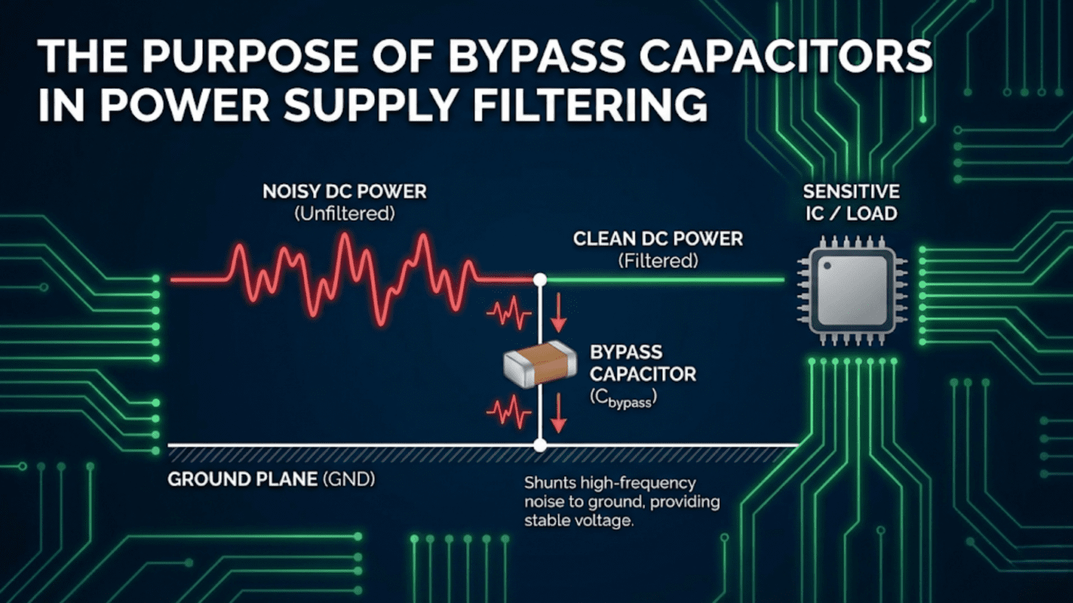
Bypass capacitors in power supply filtering serve two related but distinct roles: they filter out ripple and noise from the power supply itself (large electrolytic capacitors after the rectifier or regulator), and they bypass high-frequency noise to ground locally near each circuit section (smaller ceramic capacitors). Together, they prevent power supply voltage variations—whether from rectifier ripple, switching regulator noise, or load-induced transients—from reaching sensitive circuits. A complete power supply filter typically uses a large bulk capacitor (100μF–10,000μF) for ripple reduction, medium ceramic capacitors (1μF–10μF) for mid-frequency filtering, and small ceramics (100nF) at each IC for local high-frequency bypassing.
Introduction: Why Power Supply Quality Matters Enormously
In an ideal world, a power supply would deliver a perfectly constant, perfectly clean DC voltage regardless of what the load is doing. In reality, every power supply has limitations. Unregulated supplies from rectified AC mains have substantial voltage ripple at 100–120Hz. Switching regulators—used in most modern equipment for their efficiency—introduce switching noise at tens to hundreds of kilohertz. Even high-quality linear regulators have finite bandwidth, meaning they cannot instantaneously correct for rapid load changes. And every supply shares its output rail with multiple circuits that all create their own current variations.
These imperfections matter because every circuit connected to the supply is affected by supply voltage variations. An op-amp’s output changes slightly when its supply voltage changes (finite power supply rejection ratio). An ADC reads different values depending on its reference and supply voltages. A crystal oscillator’s frequency shifts slightly with supply voltage. A digital logic circuit’s noise margin shrinks when the supply dips below nominal. In high-speed digital circuits, supply voltage noise couples directly into signal paths and creates timing errors, data corruption, and mysterious failures.
Power supply filtering—the combination of capacitors, inductors, and in some cases active circuits placed between the power source and the circuits being powered—is the engineering response to this reality. It doesn’t make the power supply perfect; it makes the supply’s imperfections invisible to the circuits downstream.
Understanding bypass capacitor filtering at depth is transformative for practical electronics work. It explains why professional PCBs have so many capacitors scattered across them, why oscilloscopes reveal problems that multimeters hide, why some circuits work on a bench supply but fail on battery power, and why certain circuit failures disappear when the power supply is upgraded or when a few capacitors are added in the right places.
This article explores the full scope of power supply bypass filtering: what creates the noise and ripple that capacitors must remove, the physics of how capacitors filter these imperfections, the specific roles of different capacitor types and values, complete filter design for various supply types, and the practical placement strategies that make filtering effective rather than decorative.
The Sources of Power Supply Noise and Ripple
Unregulated Supplies: Rectifier Ripple
The most basic DC power supply converts AC mains voltage to DC through a transformer, rectifier, and capacitor. The rectifier converts the AC sine wave into a pulsating DC — a series of humps. The filter capacitor smooths these humps, but unless the capacitor is infinitely large (it isn’t), the voltage rises and falls with each pulse. This variation is called ripple.
Full-wave rectifier ripple: For a full-wave rectified supply with load current I_load and filter capacitor C:
V_ripple ≈ I_load / (2 × f × C)
Where f is the mains frequency (50Hz in Europe, 60Hz in North America).
Example: 12V supply, 1A load, 1000μF filter capacitor, 60Hz: V_ripple = 1A / (2 × 60Hz × 1000μF) = 1A / 0.12 = 8.33V
That’s enormous ripple — clearly a 1000μF is insufficient for a 1A load at 60Hz. Let’s solve for required capacitance for 0.5V maximum ripple: C = I_load / (2 × f × V_ripple_max) = 1A / (2 × 60 × 0.5) = 16,700μF
This explains why transformer-based supplies use very large capacitors — often 10,000μF or more — after the rectifier.
Linear Voltage Regulators: Residual Ripple and Noise
Linear regulators (7805, LM317, LM1117, etc.) significantly reduce ripple through their regulation action. A typical linear regulator has ripple rejection of 60–80dB — meaning a 1V ripple on the input appears as only 0.001–0.01V on the output.
However, linear regulators have limitations:
- Finite bandwidth: They regulate well at low frequencies but cannot correct very high-frequency variations
- Load transient response: Sudden load changes cause output voltage spikes before the regulator’s feedback loop can respond
- Internal noise: The regulator’s reference and error amplifier contribute their own small noise
The output capacitor of a linear regulator is critical for stability (prevents oscillation in the feedback loop) and for load transient response (supplies current during the brief moment before the regulator can respond).
Minimum output capacitor for linear regulators: Most linear regulators specify minimum output capacitance — typically 1μF–10μF. This is not optional: too small an output capacitor causes the regulator to oscillate. Most datasheets specify both minimum value and maximum ESR for stability.
Switching Regulators: High-Frequency Switching Noise
Switch-mode power supplies (SMPS) — buck converters, boost converters, flyback converters — operate by rapidly switching a transistor on and off, typically at 100kHz–1MHz or higher. While dramatically more efficient than linear regulators (80–95% vs. 40–60%), they introduce switching noise at the switching frequency and all its harmonics.
Switching noise characteristics:
- Fundamental frequency: 100kHz–1MHz (depends on converter design)
- Harmonics: 2×, 3×, 4× the fundamental, extending to 10MHz+
- Amplitude: Typically 10–100mV of ripple at the switching frequency on the output
A switching supply powering sensitive analog circuits or RF receivers requires substantial filtering to suppress this noise. The combination of:
- Output bulk capacitor (100μF–1000μF ceramic or low-ESR electrolytic)
- LC filter (inductor + capacitor) creating additional attenuation
- Ferrite bead + capacitor near sensitive circuit sections
…is typically needed to reduce switching noise from 50mV to below 1mV for demanding applications.
Load-Generated Noise: Circuits Creating Their Own Problems
Even with a perfect power supply, circuits generate supply noise through their own operation — exactly as described in the decoupling capacitor article. Microcontrollers, digital logic, and switching circuits create current spikes that propagate backwards into the supply rail, affecting everything else connected to the same rail.
Why this matters at the power supply level: All circuits on the same supply rail share a common impedance — the impedance of the supply traces, wires, and capacitors between them. When one circuit creates a current spike, that spike flows through the shared impedance and changes the voltage seen by all other circuits on the same rail. This is conducted interference — one circuit contaminating another through the shared power rail.
The defense: Bypass capacitors at each circuit section, ferrite beads between sections, and in extreme cases, completely separate regulated supplies for sensitive circuit sections.
The Physics of Capacitive Filtering
The Low-Pass Filter Concept
A capacitor across the supply rail (from VCC to GND) forms part of a low-pass filter. Low-pass filters pass low-frequency signals (including DC) while attenuating high-frequency signals:
RC low-pass filter: When a capacitor C is connected across the supply, and the supply has source impedance R_source (from trace resistance, regulator output impedance, etc.):
Cutoff frequency: f_c = 1 / (2π × R × C)
Below f_c: Noise passes through relatively unattenuated Above f_c: Noise is attenuated at 20dB per decade (×10 reduction per decade frequency increase)
Example: R_source = 1Ω (from trace and regulator), C = 100μF f_c = 1 / (2π × 1 × 100μF) = 1,592Hz
Above 1.6kHz: Each decade of frequency gives 20dB of attenuation At 16kHz (10× f_c): Attenuation = 20dB (10× reduction) At 160kHz (100× f_c): Attenuation = 40dB (100× reduction)
The LC Filter: Stronger Filtering
Adding an inductor in series with the supply before the capacitor creates an LC filter — more effective than RC because inductors don’t dissipate power:
LC low-pass filter cutoff: f_c = 1 / (2π × √(L × C))
Attenuation above cutoff: 40dB per decade (much steeper than RC’s 20dB/decade)
Example: L = 10μH, C = 100μF f_c = 1 / (2π × √(10μH × 100μF)) = 1 / (2π × √(10⁻⁶)) = 1 / (2π × 0.001) = 159Hz
Above 159Hz: Attenuation increases at 40dB/decade At 1.59kHz (10× f_c): Attenuation = 40dB (100× reduction) At 15.9kHz (100× f_c): Attenuation = 80dB (10,000× reduction)
LC filters are used after switching regulators where strong filtering is needed without power loss.
Why Multiple Capacitor Values Work Better Together
No single capacitor can filter the entire frequency range from 100Hz ripple to 1GHz switching noise. Each capacitor type and value has a frequency range over which it is effective:
Large electrolytic (1000μF–10,000μF):
- Effective range: DC to ~10kHz
- Handles rectifier ripple (100–120Hz) and low-frequency load variations
- High ESL makes it ineffective at high frequencies
- Self-resonant frequency: ~1–10kHz
Medium ceramic (1μF–100μF):
- Effective range: 1kHz–10MHz
- Handles switching regulator frequencies and medium-frequency supply variations
- Lower ESL than electrolytic, good up to tens of MHz
- Self-resonant frequency: ~10–100MHz depending on package
Small ceramic (10nF–100nF):
- Effective range: 10MHz–500MHz
- Handles high-frequency digital switching noise
- Very low ESL in small packages
- Self-resonant frequency: ~100MHz–1GHz
Very small ceramic (1nF–10nF):
- Effective range: 100MHz–2GHz
- Handles RF frequencies and very high-speed digital edge noise
The resulting coverage: By using one capacitor from each range, the supply impedance is kept low across the entire relevant frequency spectrum — from the 100Hz ripple down to the 500MHz digital switching noise.
Designing a Complete Power Supply Filter
Stage 1: The Mains-Derived Supply
For a transformer-rectifier supply providing 12V at 2A:
Rectifier output capacitor (C1): Target ripple: V_ripple = 0.5V (acceptable for 12V) f = 60Hz (full-wave, so 2× = 120Hz) C = I_load / (2 × f × V_ripple) = 2A / (2 × 60 × 0.5) = 33,333μF → use 33,000μF or 47,000μF
In practice: two 22,000μF 25V electrolytic capacitors in parallel.
Why such large values? Mains ripple at 60Hz (120Hz full-wave) requires enormous capacitance because the frequency is so low. This is why transformer-based linear supplies contain those large, heavy aluminum cylinders.
Stage 2: Linear Voltage Regulator Output
After a 7812 or LM317 regulator producing 12V regulated:
Output capacitor (C2, for stability): Most linear regulators specify 1μF–10μF minimum output capacitance. Low-ESR types preferred for stability. Use: 10μF ceramic or 10μF–100μF electrolytic with ESR in specified range
Output bypass (C3, for high-frequency noise): The regulator’s rejection ratio falls at high frequencies. Use: 100nF ceramic placed near the regulator output pin
Input capacitor (C4, for transient support): Prevents the regulator input voltage from drooping during sudden load increases. Use: 100nF–10μF ceramic near regulator input pin
Complete linear regulator filter:
Transformer/Rectifier
       │
   [C1: 33,000μF/25V electrolytic]  ← Ripple filter
       │
   [7812 Regulator]
       │
   ┌───┤
   │  [C2: 10μF electrolytic]       ← Stability capacitor
   │  [C3: 100nF ceramic]           ← HF bypass
   │   │
└───┴───── To circuits (12V regulated)Stage 3: Point-of-Load Filtering for Sensitive Circuits
If the 12V rail powers a mix of digital and sensitive analog circuits, add additional filtering before the analog section:
Ferrite bead filter:
12V Rail (shared with digital)
       │
   [Ferrite bead: 600Ω @ 100MHz, rated 500mA]
       │
   [C4: 10μF ceramic]   ← Bulk for analog section
   [C5: 100nF ceramic]  ← HF bypass for analog section
       │
Analog circuits (12V, filtered)Per-IC decoupling (final stage): At each IC:
Filtered 12V rail ─────── IC VCC pin
                     │
                 [100nF ceramic]  ← Immediate IC decoupling
                     │
GNDFiltering for a Switching Regulator Output
A buck converter (e.g., LM2596 providing 5V from 12V) has more complex filtering requirements:
Output capacitor (specified by regulator IC): Most buck converter ICs specify output capacitance range for stability. Typical: 100μF–470μF electrolytic or ceramic with specific ESR range
Low-ESR electrolytics (105°C rated polymer types) or large ceramic capacitors preferred over standard electrolytics for lower output ripple.
Additional LC filter for sensitive applications: After the buck regulator’s own output capacitor:
Buck converter output
       │
   [L1: 4.7μH ferrite inductor, rated for load current]
       │
   [C6: 100μF ceramic or low-ESR electrolytic]
   [C7: 10μF ceramic]
   [C8: 100nF ceramic]
       │
Sensitive circuits (5V, switching noise filtered)The additional LC filter can reduce switching noise from 50mV to under 1mV — often necessary for RF circuits, precision ADCs, and microphone preamps powered from switching supplies.
Capacitor Selection for Filtering
Electrolytic Capacitors: Bulk Ripple Filtering
Key specifications for electrolytic filter capacitors:
Capacitance: Determined by ripple calculation. For mains-derived supplies, typically thousands of μF.
Voltage rating: Must exceed the maximum supply voltage including ripple. For 12V supply, use 25V-rated capacitors (not 16V — insufficient margin). Rule of thumb: 2× nominal voltage.
ESR (Equivalent Series Resistance): Low-ESR capacitors (often labeled “105°C” or “low impedance” or using polymer electrolyte) have dramatically lower ESR than standard types:
- Standard electrolytic: ESR = 0.5–5Ω
- Low-ESR electrolytic: ESR = 0.05–0.5Ω
- Polymer electrolytic: ESR = 0.01–0.1Ω
Low ESR matters because:
- Less voltage drop across the capacitor during high-current transients (better ripple filtering)
- Less power dissipated in the capacitor (lower temperature = longer life)
- More stable over temperature
Ripple current rating: The RMS current through a filter capacitor causes self-heating. Exceeding the ripple current rating shortens capacitor life dramatically (electrolytic capacitor life approximately halves with every 10°C temperature increase). Always verify the ripple current rating, especially in switching supply designs.
Temperature coefficient: Standard electrolytic capacitors lose capacitance significantly at cold temperatures (-40°C: may be only 50% of room temperature value). High-temperature rated capacitors are more stable.
Ceramic Capacitors: Voltage Coefficient Derating
Ceramic capacitors have an important non-ideal behavior often overlooked by beginners: their capacitance decreases with applied DC voltage. This is called DC bias derating and is most significant for Class II ceramics (X5R, X7R, Y5V).
Example of DC bias derating: A 10μF X5R ceramic capacitor rated 10V may have only 3–5μF of actual capacitance when charged to 5V, and perhaps 1–2μF when charged to its rated 10V.
Why this matters for filtering: If you design a filter requiring 10μF and choose a 10V-rated 10μF X5R capacitor for a 9V supply, you may actually have only 2–3μF — insufficient for your design.
Solutions:
- Use capacitors with higher voltage ratings than necessary (a 10μF 25V capacitor on a 5V supply will retain much more capacitance than a 10μF 10V capacitor)
- Use C0G/NP0 dielectric for applications requiring stable capacitance (though C0G is limited to small values, typically ≤100nF)
- Verify with datasheet bias derating curves, not just nominal values
Tantalum Capacitors: The Niche Case
Tantalum capacitors offer moderate ESR, compact size, and good stability but with critical failure modes:
- Reverse voltage: Even momentary reverse voltage can destroy tantalum capacitors catastrophically (fire, not just failure)
- Voltage rating margin: Tantalums should be derated to 50–70% of their voltage rating in normal use
- Surge current: Tantalums can fail if powered through a low-impedance source without current limiting
Use tantalums only where size matters and reverse voltage and surge are carefully controlled. For most filter applications, ceramic or electrolytic are safer choices.
Special Filtering Situations
Mixed Analog-Digital Circuits: Split Supply Rails
When analog and digital circuits share a PCB, their supply rails should be filtered separately to prevent digital noise from contaminating analog circuits.
Ground plane strategy: Use a single, solid ground plane (not split ground). This provides the lowest impedance current return paths. Ground splitting creates more problems than it solves in most designs.
Supply filtering strategy:
- Single main supply connects to both analog and digital bypass networks
- Ferrite beads separate analog supply from digital supply at the point where they diverge
- Each section has its own complete bypass network
Main 3.3V supply
        │
    ┌───┴────────────────────────────────────┐
    │                                        │
[Ferrite]                             [Direct connection]
    │                                        │
[10μF C][100nF C]              Analog     Digital circuits
                               circuits   [10μF][100nF each IC]
Analog supply (quiet) [per IC: 100nF]RF and High-Frequency Circuits
Radio frequency circuits demand the most careful supply filtering because:
- High-frequency noise on the supply couples directly into the RF circuitry
- Even millivolts of supply noise create intermodulation products that degrade receiver performance
- The circuits themselves operate at the very frequencies that need to be kept off the supply rails
RF supply filtering approach:
- Low-frequency bulk: 100μF–470μF near supply entry point
- Mid-frequency: 10μF ceramic
- High-frequency: 100nF ceramic immediately at IC
- RF-frequency: 10nF and 1nF ceramics immediately at each RF supply pin
- λ/4 stub bypass (advanced): At specific frequencies, a quarter-wavelength open stub acts as a short circuit at that frequency — used in microwave circuit supply filtering
Separate regulators: Many RF designs use completely separate linear regulators for VCO (voltage-controlled oscillator) supply and receive chain supply, with filtering after each.
Audio Circuits: Defeating Hum and Hiss
Audio circuits are sensitive to:
- 60Hz/50Hz hum: From power supply ripple at mains frequency
- 100Hz/120Hz hum: Full-wave rectifier ripple
- Higher harmonics: Up to kilohertz range from rectifier and regulator
- Switching noise: From switching supplies (kHz range)
Audio supply filtering: A regulated supply with good filtering reduces hum to acceptable levels. The key specifications for audio:
- Power supply rejection ratio (PSRR) of op-amps used
- Ripple voltage on supply rails
- Noise spectral density of the regulator
Practical audio supply:
- Linear regulator strongly preferred over switching (no switching noise in audio band)
- 1000μF–10,000μF bulk capacitor after rectifier
- Linear regulator (LM317, LM337 for negative rail)
- 100μF electrolytic + 100nF ceramic at regulator output
- 100nF ceramic + 10μF ceramic at each op-amp supply pin
- Low-dropout (LDO) linear regulators have better PSRR than standard types
Comparison Table: Filter Capacitor Roles and Selection
| Filter Stage | Capacitor Type | Typical Value | Location | Primary Role | Frequency Range |
|---|---|---|---|---|---|
| Rectifier output | Electrolytic | 1,000μF–47,000μF | After rectifier diodes | Mains ripple reduction | 50–120Hz |
| Regulator input | Ceramic or electrolytic | 100nF–10μF | Near regulator input pin | Transient support, stability | 100Hz–10MHz |
| Regulator output (stability) | Low-ESR electrolytic or ceramic | 1μF–100μF | Near regulator output pin | Regulator stability, transient response | DC–1MHz |
| Regulator output (HF) | Ceramic (MLCC) | 100nF | Near regulator output pin | High-frequency noise bypass | 1MHz–500MHz |
| PCB power rail bulk | Electrolytic or large ceramic | 47μF–470μF | At supply entry to PCB | Shared rail decoupling | 1kHz–1MHz |
| Section filter (ferrite+cap) | Ceramic | 10μF + 100nF | Between circuit sections | Cross-contamination prevention | 1kHz–500MHz |
| Per-IC bypass | Ceramic (MLCC) | 100nF | Adjacent to IC power pin | IC switching noise | 10MHz–500MHz |
| High-speed IC bypass | Small ceramic | 10nF + 1nF | On IC power pin (SMD) | Very-high-frequency switching | 100MHz–2GHz |
| RF supply bypass | Ceramic (smallest pkg) | 100pF–1nF | On RF IC supply pin | RF frequency bypassing | 500MHz–5GHz |
Practical Troubleshooting: Diagnosing Power Supply Noise
Equipment Needed
Oscilloscope with 100MHz+ bandwidth: Essential for seeing high-frequency supply noise. Set to AC coupling to reject the DC level and see only variations.
Low-inductance probe technique: Remove the standard probe tip and ground clip. Instead, use the probe tip directly on the supply node and use the ground collar/spring directly on the nearest ground. This eliminates the ground clip inductance (~10–50nH) that would otherwise add a significant antenna effect.
Step-by-Step Diagnosis
Step 1: Measure supply noise at the regulator output Connect oscilloscope (AC-coupled, 50mV/div, 10μs/div) directly at the regulator output pins. Note noise amplitude and character.
- Periodic at power line frequency: Ripple problem (insufficient bulk capacitance)
- Periodic at 100kHz–1MHz: Switching regulator noise (insufficient output filtering)
- Random high-frequency bursts: Load-induced transients (insufficient decoupling at affected ICs)
Step 2: Trace noise source Move probe to different points on the power rail. Noise level should decrease as you move further from the source.
Step 3: Check existing capacitors Physically verify decoupling capacitors are present and correctly placed. A capacitor visible on the schematic but not placed on the PCB, or placed far from the IC, provides no benefit.
Step 4: Add capacitors and observe improvement With a physically accessible board, temporarily add capacitors by hand (touching them to power and ground pins) and observe whether noise decreases. If it does, permanent capacitors at those locations will fix the issue.
Common Symptoms and Fixes
Symptom: ADC gives noisy readings even with stable input signal Cause: Supply noise on ADC reference or VCC corrupting conversions Fix: Add ferrite bead + 100nF + 10μF between main supply and ADC/microcontroller VCC; add separate 100nF on VREF pin
Symptom: RF receiver desensitization when other circuits operate Cause: Digital or switching noise coupling into RF supply Fix: Separate linear regulator for RF section; LC filter + 100nF at RF IC supply pins
Symptom: Audio hum proportional to load current Cause: Insufficient bulk capacitance; too much ripple after rectifier Fix: Increase rectifier filter capacitor size; verify no shared ground path between high-current and sensitive circuits
Symptom: Microcontroller resets during high-current load switching Cause: Supply voltage dip below brownout threshold when large load starts Fix: Increase bulk capacitance at MCU supply; add ferrite bead to isolate MCU supply from high-current load supply
Conclusion: Filtering as Systematic Engineering
Power supply bypass filtering is not a collection of arbitrary rules — it is a systematic engineering response to the physical realities of power supply imperfection and circuit sensitivity. Every element of a complete filter serves a specific purpose at a specific frequency range, and the combination of elements provides the clean, stable supply voltage that all circuits require to function correctly.
The Hierarchy of Filtering
Level 1 — At the source (transformer or switching supply): Large bulk capacitors reduce raw ripple to a manageable level. This is the heaviest lifting — removing the majority of the mains-derived ripple and providing the gross energy storage needed for load variations.
Level 2 — At the regulator: Input and output capacitors ensure regulator stability and improve transient response. The regulator itself provides active filtering through its regulation action, but it needs proper capacitors to work correctly.
Level 3 — At the PCB (section filtering): Medium-value ceramics and ferrite beads prevent cross-contamination between circuit sections. This is where analog-digital isolation happens — keeping switching noise out of measurement circuits.
Level 4 — At each IC (local decoupling): Small ceramics immediately adjacent to IC power pins handle the highest-frequency components of the supply noise — the nanosecond-scale current spikes from IC switching activity that no regulator or bulk capacitor can address.
The Investment Perspective
Bypass capacitors are inexpensive — a cent or two each at most. The PCB area they occupy is modest — a few square millimeters for the complete set around an IC. The time to add them properly is minutes. The cost of omitting them — hours or days of mysterious debugging, unreliable products, customer returns, failed EMC testing — is incomparably higher.
Professional engineers add bypass capacitors automatically, without calculating whether they’re “necessary.” They do this not out of habit or superstition but because experience has taught them the cost of omission. The capacitors always earn their keep.
Understanding why — understanding the ripple calculation, the frequency-dependent impedance, the role of ESR and ESL, the importance of physical placement — transforms this habit from rote rule-following into informed engineering practice. And informed engineering practice is what produces circuits that work reliably, consistently, and correctly — the first time and every time.
The capacitor that bypasses noise to ground is, in a very real sense, protecting the integrity of every signal in your circuit. It is quiet infrastructure, invisible in operation, noticed only in its absence.