
The European Union officially launched its €2.5 billion NanoIC pilot line on February 9, 2026, representing one of the most significant milestones in the EU Chips Act programme aimed at doubling Europe’s global semiconductor market share from approximately 10% to 20% by 2030. The initiative establishes state-of-the-art research and manufacturing infrastructure enabling European companies and institutions to develop, prototype, and validate advanced chip designs without relying exclusively on fabrication facilities in Taiwan, South Korea, and the United States.
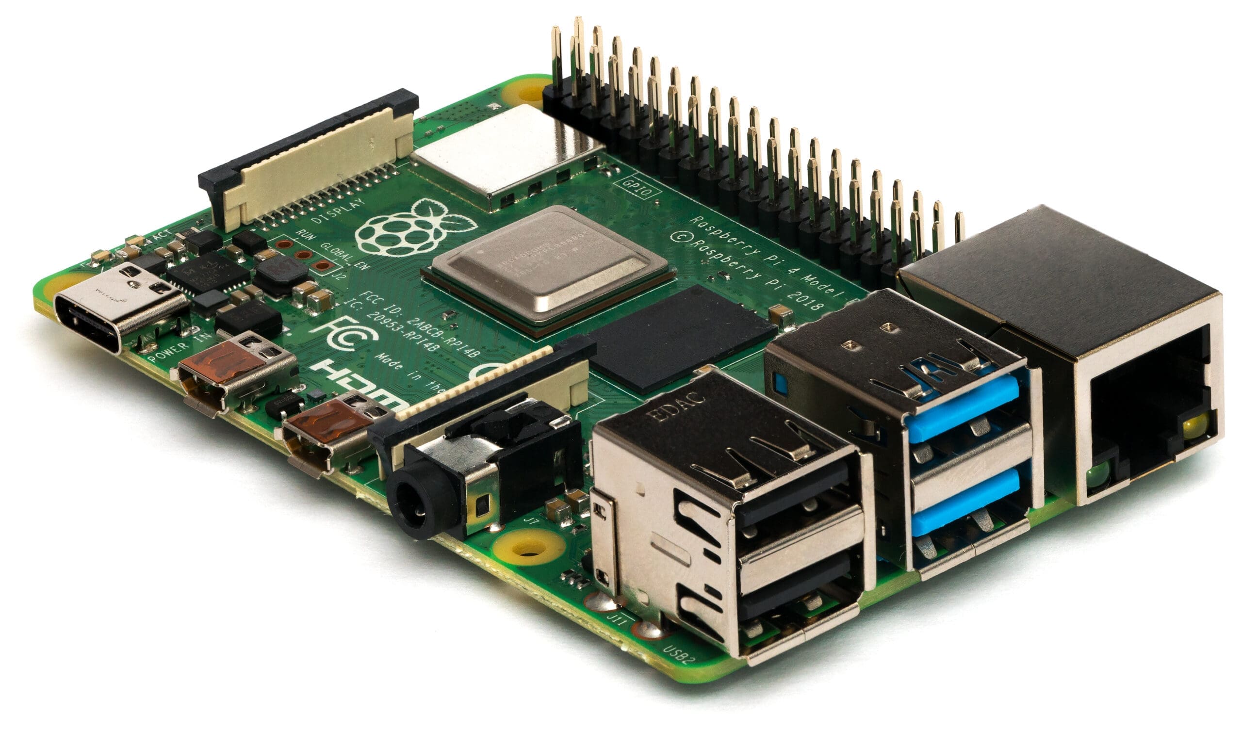
The NanoIC pilot line is designed to bridge a persistent gap in Europe’s semiconductor ecosystem. While the continent is home to world-class chip design companies including ASML, Infineon, NXP, STMicroelectronics, and ARM (now independent), it has historically lacked domestic fabrication capacity for the most advanced process nodes. This creates vulnerability: European companies must send cutting-edge chip designs to foreign foundries where geopolitical tensions, export controls, and capacity constraints introduce supply chain risks increasingly unacceptable for defence, automotive, and critical infrastructure applications.
The pilot line targets several advanced technology areas. Advanced packaging techniques enabling chiplet architectures are a priority, allowing multiple specialised chips to be integrated into unified systems with performance approaching monolithic designs. Novel semiconductor materials including gallium nitride and silicon carbide, which enable superior efficiency in power electronics and radio frequency applications, are central research areas. Advanced lithography processes and new transistor architectures required for sub-3 nanometre devices represent the frontier capability the programme ultimately aims to develop.
The funding structure combines EU contributions from the Chips Act budget, co-investment from member state governments particularly Germany, France, and the Netherlands, and industry partnerships with semiconductor companies committing research resources and engineering talent. The distributed governance model reflects the challenge of coordinating semiconductor investment across EU members with different industrial bases, regulatory environments, and national priorities.
Industry stakeholders have responded positively to the announcement while noting that pilot lines represent only the beginning of a longer journey to competitive manufacturing. Building full-scale advanced fabrication facilities requires tens of billions of euros beyond what pilot lines provide, sustained government commitment over decade-long timeframes, and attraction of semiconductor engineering talent that Europe currently lacks in sufficient quantities.
The geopolitical urgency driving NanoIC stems from lessons learned during the 2021-2022 chip shortage that paralysed automotive manufacturing across Europe, and from growing concern about Taiwan Strait tensions that could disrupt access to TSMC’s leading-edge fabs. The European Commission has explicitly linked semiconductor sovereignty to broader strategic autonomy objectives — ensuring that critical technologies for defence, electric vehicles, renewable energy, and AI remain accessible regardless of geopolitical developments.
For AI specifically, advanced chips manufactured within Europe would enable training and deploying AI models subject to EU regulations without transferring sensitive data or algorithmic IP to jurisdictions with different legal frameworks. This regulatory alignment benefit complements the security rationale.